


In the world of printed circuit board (PCB) manufacturing, the devil is in the details. Even subtle design features like plated edges, castellated holes, and advanced milling techniques have far-reaching implications in terms of cost and production time.
In this blog post, we will delve into some of these special features to help PCB designers and engineers understand the complexities involved and the consequential impact on manufacturing costs.

Plated Edges and Castellated Holes
Plated edges are often used in specialized applications such as edge connectors where the edges of the PCB interact directly with another hardware component. This plating on the edge enhances the electrical conductivity and mechanical strength, but doing so involves multiple additional processes. Initially, the edge has to be prepared and cleaned meticulously, which requires a precise alignment in the manufacturing workflow. The plating itself involves a separate chemical process, requiring its own set of tools and safety measures. Post-plating inspection is also essential to ensure that the coating is uniform and meets the specified requirements.
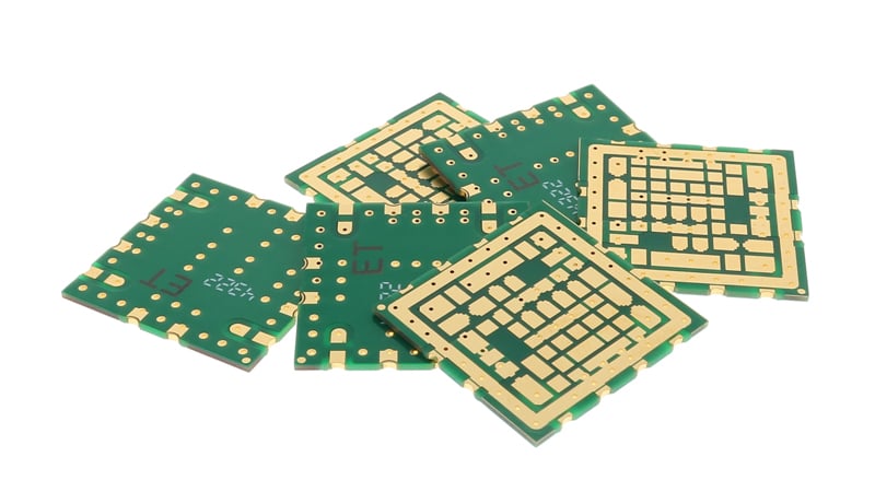
Example of circuit boards with plated edges.
Castellated holes, on the other hand, offer a unique design element that allows the PCB to be soldered directly onto another board. They appear at the edge of the board, essentially looking like a turret in a castle, hence the name "castellated." But this aesthetic and functional benefit comes at a cost. The holes have to be precisely drilled, and then a part of the hole is cut off when the board is profiled. This half-hole is then plated, usually with a metal like copper, to ensure good electrical conductivity.
Both features require specific tooling and settings in the drilling machines used. The drilling parameters, such as speed, pressure, and bit type, often differ from the standard settings, demanding a separate setup and thereby increasing the manufacturing time. Following the drilling, additional checks are necessary to ensure the accuracy of these features, which might also entail image swaps. An image swap in this context means changing the film that represents the layer of the board to ensure that areas around the plated edges or castellated holes will hold up during the entire manufacturing process. This is crucial because any flaws in these specialized features could lead to electrical issues, like poor connectivity, or mechanical problems, such as structural weaknesses, in the final product.
Primary Routing and Drilling
When it comes to primary routing and drilling, it's a finely orchestrated sequence of tasks that serves specific manufacturing requirements. Drilling holes along the edge of the PCB is a fairly straightforward affair, guided by precise machinery and established procedures. But when primary routing enters the equation, the complexity scales up. Unlike traditional drilling, primary routing involves creating a smooth channel along the board's edge, which serves a range of applications from heat dissipation to specialized component housing.
If this channel also requires plating, for either conductivity or durability, additional steps must be taken before the circuit board proceeds further down the manufacturing line. The plated channel must be prepared for the primary image, the etched design that defines the PCB's conductive pathways. This is a crucial step, as the primary image lays the groundwork for the rest of the manufacturing process. Often, this necessitates a film swap, which means replacing the layer film that is used as a template for etching the PCB. The purpose of this swap is to make sure that the plating in the routed channel will not compromise the integrity of the primary image.
This film swap isn't just a simple exchange; it requires recalibration of the equipment and may also demand quality checks to ensure that the new film aligns perfectly with the existing features on the board. Each of these additional steps, though they may seem minor, incrementally adds to the manufacturing time and therefore, the cost. Mistakes at this stage can be costly, leading to delays or, worse, requiring the scrapping of the board, making the attention to detail paramount.
In essence, while primary routing and drilling may appear as minor alterations in the grand scheme of the manufacturing process, their impact on the workflow and cost structure is significant. Whether it’s specialized tooling or the additional quality checks and film swaps, these features require comprehensive planning and execution. It's a ripple effect where a single change in design can cascade into multiple layers of engineering and manufacturing complexity. But, as with many things in engineering, the devil is in the details, and it's these details that can make all the difference in the final product.
Milling and Excessive Routing
Milling and excessive routing add another layer of complexity. Milling shapes the circuit board's size and form, while controlled-depth routing removes material from the board’s top side, often to make space for specific components.
The time consumed for programming, handling the specialized equipment, and actual processing are all additional costs that need to be factored in. Excessive routing, involving constant lifting and plunging of the drill, can take an inordinate amount of time, especially for large batches, tying up valuable equipment and labor.
Counterbore, Countersink, and Back Drilling
When we talk about counterbore, countersink, and back drilling, we're diving into some of the more intricate facets of PCB manufacturing that often go unnoticed but play a critical role in a circuit board's utility and performance. Counterbore holes are typically cylindrical and designed to allow the head of a screw to sit flush with or below the surface of the board. Countersink holes, in contrast, are conical and allow for screws with a tapered head to sit flush with the surface. While these features enable secure mounting of the PCB, they require specialized drill bits and tooling settings, and, occasionally, custom tooling may even have to be acquired, adding an extra step of procurement to the process.
It's not just about drilling the hole and moving on; the type of hole, whether it's a counterbore or countersink, often requires careful planning to ensure compatibility with the screws or fasteners to be used. The decision between plated and non-plated versions also comes into play, affecting the subsequent manufacturing steps. Should the holes be plated for increased conductivity, another layer of complexity is added, requiring separate treatment and quality checks to ensure proper plating thickness and uniformity.
Back drilling adds yet another layer to the conversation. Unlike counterbores and countersinks, which are generally a one-step process in the drilling phase, back drilling is a two-step operation aimed at removing any unnecessary internal plating within a hole. After the primary hole is drilled and plated, a secondary drilling operation removes the plating from certain inner layers of the board. This process demands meticulous engineering planning to generate the programs for both the primary and secondary drilling.
But the intricacy doesn't stop at planning; it extends into execution. The process of drilling the same hole twice raises the stakes in terms of quality control. Any misalignment or variance in the secondary drilling can risk scrapping the entire board, leading to wasted materials and time. As such, back drilling not only demands more engineering time for program development but also introduces an element of risk that needs to be meticulously managed.
Cavity Boards
Cavity boards are not just another PCB variant; they are a testament to the advances in engineering and material science, particularly in more complex applications like embedded components or advanced thermal management. These boards are primarily composed of FR4 and polyimide materials, and often feature a labyrinth of different layers, each requiring its own specific routing. The manufacturing process for these boards requires a certain type of prepreg material that's either no-flow or low-flow to prevent any residue from contaminating the board during the lamination process.
The tight tolerances associated with these boards, often in the realm of plus or minus 5 mils, place a high demand on the precision of both the materials used and the machinery tasked with shaping them. It's a high-stakes game where even the smallest error can lead to costly reworks or, in the worst case, scrapping the board altogether. The sum of these complexities makes cavity boards a more labor-intensive and resource-demanding endeavor, often translating into higher production costs and longer lead times. It's a classic case of how higher complexity requires higher investments in time, expertise, and specialized materials to ensure a product meets its design specifications and performance criteria.
Summary
From plated edges to cavity boards, each unique feature added to a PCB design has a cascading effect on the overall manufacturing cost. They demand specialized tools, additional labor, and extra engineering time, and they tie up equipment that could be used for other jobs. As a PCB designer or engineer, understanding the implications of these features allows for better planning and decision-making, ensuring that the final product meets specifications without breaking the bank.
In a rapidly evolving industry where design complexity is increasing, it's crucial to weigh the benefits and challenges of incorporating such specialized features into your PCB designs. Keep in mind that these features, while enhancing the board's capabilities, come with their own set of costs and complexities.
Understanding these nuances is key to efficient, cost-effective PCB design and manufacturing. After all, in engineering as in life, knowledge is power.
Key Takeaways
- Plated edges and castellated holes improve conductivity and functionality but require additional drilling, plating, and inspection steps, which raise both cost and lead time.
- Primary routing and drilling add complexity when channels or edges must be plated, often requiring film swaps and recalibration, which increases engineering and manufacturing effort.
- Milling and excessive routing consume significant machine time and programming, especially in large runs, adding cost due to extended handling and equipment use.
- Counterbore, countersink, and back drilling enable secure mounting and signal reliability but require specialized tooling, multiple drilling steps, and careful alignment, making them higher-risk and more expensive.
- Cavity boards demand tight tolerances, special prepregs, and precise multi-layer routing; while highly functional for advanced applications, they are labor-intensive and increase both cost and lead time.


