


Having been involved in the printed circuit board (PCB) world for nearly four decades, I continue to see the same drawing mistakes. When declaring PCB tolerances in any given design, the PCB designer must take into consideration the manufacturing of the board itself. In this blog post, we will review some of the issues we commonly see in PCB designs that are not allowing the proper tolerances for the routing, drilling, and plating processes.

Drilling
We cannot yet have a standard plated hole size with a finished tolerance of +/-0.001”. I still see drill charts with +/-0.000” or +/-0.001” tolerances for finished holes. For a standard plated through hole, the hole size drilled needs to be about 0.006” larger than the finished size to allow for 0.0008” to 0.001” copper to be plated within the hole.
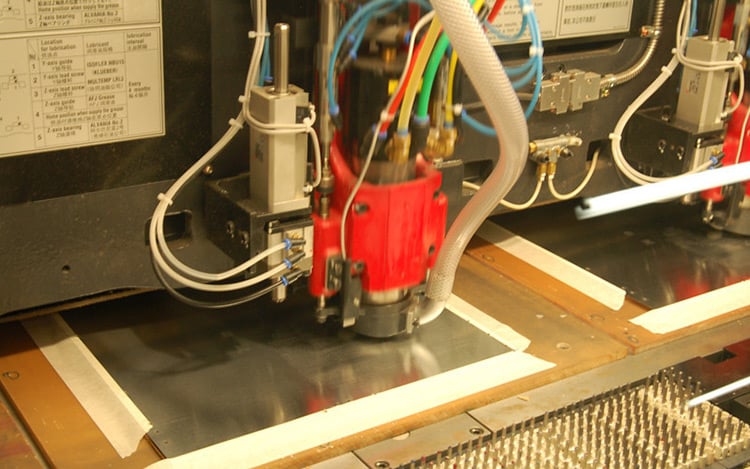
Example of a CNC drilling machine.
The table on which the PCB sits holds the boards down within very little movement. “Drill wander” does occur, however. Thus, the need for tolerances can be critical for these processes. When a large volume of circuit boards are ordered, manufacturing will stack the production panels on top of each other. Typically, there may be three panels on top of each other held down on the drill table. So, if there are four drill heads, set up with the tools required to drill the pre-plated holes, and three panels held down under each drill head that would be 12 production panels drilled at a time. This process must be done for efficient use of production time.
The problem with the above scenario is that the drill bit must now drill through a backer board used to cut down on drill smear and burrs. The drill then goes through three production panels of 0.062” FR4 or some other material. If the drill bit is not quite as sharp as a new bit, the drill size will already be off from nominal. Also, to add to that, if any of the three stacked panels has moved at all, the drill registration may be off a little, but also the drill size will not be nominal as well as the head moves up and down. Already, that +/-0.000” or +/-0.001” tolerance is blown, which is not even for the finished size.
Video: Lenz DLG-550 in Action: High-Speed, High-Accuracy PCB Drilling
Routing
For hole sizes at 0.250” and larger, the drilling becomes more of a mechanical process, which leads you to routing. The routing process of a PCB requires even more tolerance than drilling.
If a circuit board design needs a 0.250” finished plated hole, a router would need to cut open a 0.256” diameter opening for a plated hole, which itself would be at a +/-0.004” tolerance. In this scenario, the finished 0.250” size would need preferably a +/-0.005 tolerance”. Again, besides the chemistry having variables, the size of the hole adds in another variable. Basically, small holes plate faster than large holes.
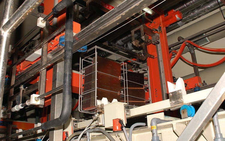
Example of a CNC PCB routing machine.
The PCBs are held down to the table with very little board movement. However, with router bit wander, plus the tolerances of the router bit itself, final size tolerance is required, preferably +/-0.005”. Also, as previously mentioned, when mass production volumes are required, the panels will be stacked more than one high. If any shift in this panel stack occurs, the final routed size will be affected.
Slots and cutouts, plated or not, required that same router tolerance on them. As router bits are used, they wear down, and the openings they cut get smaller. This is especially true in a production environment where heavy routing use is required.
Chemical Plating
As the copper is plated, the hole size will shrink down to the finished size. Plating is not an exact science so a +/-0.001” tolerance is not practical. The +/-0.003” tolerance on hole sizes up to 0.249” is preferred.
The copper plating process relies on time in the plating tanks, temperature of the tanks, and the amps of current sent into the circuit boards. A standard plating time takes from 45 minutes to an hour and a half to get enough copper into the holes. Because of the chemistry variables, along with time in the plating tanks, the temperature of the tanks, as well as the amps involved, the finished size of the plated holes needs that tolerance of +/-0.003”.
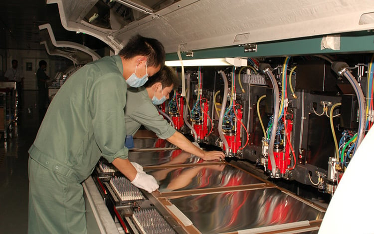
Example of PCB copper plating equipment.
Circuit board production panels come into the copper plating department after the circuit images are present and the holes have been pre-plated. The PCB panels go through a cleaning process, which again will slightly etch the hole sizes. Before the panels are placed into the copper plating tanks, several variables must be calculated.
The area that needs to be copper plated must be calculated in order to know how much amperage to send through the chemistry without “burning” the boards. The production panels must be racked in such a way to even out the current flow as much as possible. It is important for the customer to let the PCB fabricator know what plated hole tolerance is allowed and how much copper in the holes is required.
Press fit holes, where components must be pushed into the holes for a tight fit, usually have a +/-0.002” tolerance. This is about the tightest tolerance that the plating department needs to see. With that tolerance, IPC 0.0007 mils in the holes is preferred. With that, it is much easier to get those press fit holes plated down to within that +/-0.002” tolerance, plus all the +/-0.003” holes will also be in tolerance. When a customer requires 0.001” minimum in the holes, which is seen on so many drawings, it becomes more difficult in plating to be within that +/-0.002” tolerance as the panels must stay in the plating tanks that much longer.
A side note on that 0.001” requirement, many of these engineering notes came from the days when PCB designers required “1-ounce plated copper.”
One-ounce copper is actually 0.0014,” but has evolved into that 0.001” requirement. IPC class 2 only requires 0.0007”, while IPC class 3 requires 0.0008” in the holes. Most times, that 0.001“ is really not needed. A way around this requirement would be for drawings to have a note such as: “0.001” average in the holes.” That small note from the PCB engineer greatly helps production in meeting the plated hole tolerances of +/-0.002” and +/-0.003”.
Slots and Cutouts
Another factor that affects the plating process meeting the proper drilling tolerances are slots and cutouts. Slots and large plated cutouts and holes behave differently within the plating process. The chemistry must flow through all the plated holes. This is achieved by the panels moving back and forth within the tanks, and air agitation moving the chemistry around, keeping it evenly mixed. Although chemistry has a more difficult time flowing through small holes, small holes still plate faster. The large holes and slots, even though the chemistry easily flows through, plate slower.
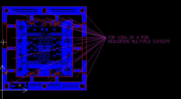
Example of a top view of a PCB requiring multiple cutouts.
If a drill chart calls for plated holes at +/-0.002” and has slots and large cutout plated areas with only a +/-0.003” tolerance, causes a plating nightmare. When the +/-0.002” holes are plated down to +/-0.002” to the finished required size, the slots and large plated cutouts are only at the upper end of the tolerance. Thus, it is better if the holes have a +/-0.003” tolerance, and the slots and cutouts have +/-0.005”, then all the holes and cutouts can be plated down into nominal finished sizes.

Summary
Tolerances on circuit board drawings are required for the best processing of the product. Having the appropriate tolerance for plated and non-plated features is very relevant. Routed features require their own larger tolerance. For smooth product flow, and faster turnaround after an order is placed, the best tolerances are a great aid. Even a small note from an engineer such as “process per IPC guidelines” will generally give you +/-0.003” on plated holes, +/-0.002” on non-plated holes, and +/-0.005” on routed features. Keeping to these guidelines is a rule of thumb that will give you a fine PCB product, ready for assembly.
Key Takeaways
- Drilling tolerances must account for drill wander and production variables: Standard plated through holes require a drilled hole size approximately 0.006” larger than the finished size to accommodate plating, and tolerances of +/-0.000” or +/-0.001” are unrealistic in high-volume manufacturing.
- Routing tolerances need to be larger than drilling tolerances: For holes larger than 0.250”, routing is used instead of drilling, requiring a tolerance of +/-0.005” due to router bit wear, bit wander, and potential misalignment in stacked panel processing.
- Chemical plating tolerances depend on process variables: The copper plating process is affected by tank temperature, plating time, and current flow, making a finished hole tolerance of +/-0.003” ideal for standard plated holes and +/-0.002” for press-fit holes.
- Larger plated slots and cutouts require higher tolerances than small holes: While small holes plate faster, large plated slots and cutouts require more time, making it essential to specify tolerances of +/-0.005” for slots and large cutouts, compared to +/-0.003” for smaller plated holes.
- Following IPC guidelines ensures realistic tolerances and manufacturability: A simple engineering note stating “process per IPC guidelines” helps maintain practical tolerances of +/-0.003” on plated holes, +/-0.002” on non-plated holes, and +/-0.005” on routed features, ensuring smoother PCB fabrication.


