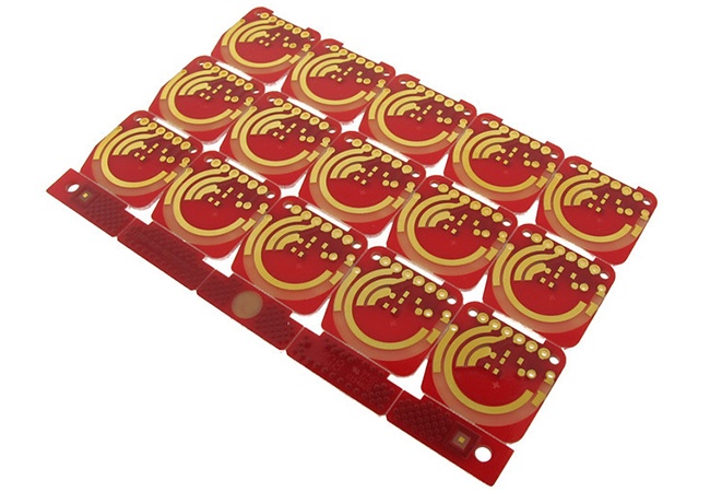
As printed circuit boards (PCBs) progressed, requiring their functions to be more and more complex and diverse, the number of layers increased from 1-2 layers, up to 4-30 layers, with 4-12-layer boards being more typical.
Read MoreJim Marsh

Recent Posts
Having been involved in the printed circuit board (PCB) world for nearly four decades, I continue to see the same drawing mistakes. When declaring PCB tolerances in any given design, the PCB designer must take into consideration the manufacturing of the board itself. In this blog post, we will review some of the issues we commonly see in PCB designs that are not allowing the proper tolerances for the routing, drilling, and plating processes.
Read MoreIn the rigid printed circuit board (PCB) world, you can easily generate a quote with cookie cutter specs, such as 0.062” thick, with FR4, green soldermask, and white silkscreen. With those standard specifications, you could quote a huge number of rigid PCBs.
Read MoreIn front-end engineering, we must gather as much manufacturing information as possible from the printed circuit board data we receive. This includes customer service notes, customer emails, and the general spec, if available. Usually there is enough information to release a printed circuit board (PCB) package to manufacturing. However, I have found many gray areas that haunt our engineering department.
Read MoreThe reason printed circuit boards (PCBs) require a surface finish rather than being left as simply bare copper is because while copper is an excellent conductor, leaving it exposed will cause it to oxidize and deteriorate over time. The increased exposure will cause the PCB to fail much sooner than expected.
Read More


