


Wrap plating is a technique used in the manufacturing of printed circuit boards (PCBs) to create a conductive layer that connects the layers of the PCB together. The process involves plating copper onto the walls of through-holes and vias in the PCB, which are then used to make electrical connections between the layers.
The term "wrap" refers to the fact that the copper layer is wrapped around the edge of the hole or via, creating a continuous electrical connection between the layers of the PCB. This is in contrast to other plating techniques, such as "blind via" or "buried via" plating, which does not extend all the way through the PCB and is used to make connections between specific layers.
Wrap plating is commonly used in multi-layer PCBs where multiple layers of copper traces are separated by insulating layers. By using wrap plating, the vias, and through-holes in the PCB can be used to create a continuous electrical path between the layers, reducing the number of wires or other connectors needed to make connections between the layers. This helps to improve the reliability and performance of the PCB, while also reducing its size and weight.

Copper wrap plating is a critical process in the manufacturing of printed circuit boards (PCBs). It involves the deposition of a thin layer of copper around the edges of a drilled hole in the PCB substrate to create a conductive path between layers of the board. In this blog post, we will discuss the importance of copper wrap plating in PCBs and how it is achieved.
PCB Wrap Platting Processes and Requirements
The need for copper wrap plating arises because the edges of a drilled hole in a PCB substrate are typically non-conductive. If left untreated, these edges could impede the flow of electrical current between layers of the board, leading to poor signal integrity and unreliable operation. Copper wrap plating solves this problem by creating a conductive path between layers of the PCB, ensuring that electrical signals can flow freely throughout the circuit.
In terms of wrap plating requirements for via-in-pad structures, IPC-6012B states that wrap plating is required for all vias that are in contact with a surface mount pad or hole pad. The wrap plating should extend a minimum of 0.025mm (1mil) up the sidewall of the hole or via, and it should provide a continuous electrical connection between the pad and the internal conductive layers of the PCB.
Furthermore, IPC-6012B specifies that the plating should be visually inspected to ensure that it completely covers the sidewalls of the vias and that there are no voids or thin spots. The thickness of the wrap plating should also be measured and verified to meet the specified requirements.
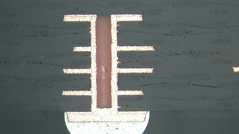
Example of good wrap plating.
PCB Electroplating Process
Electroplating is a process of depositing a thin layer of metal onto a substrate using an electric current. It is a widely used technique in various industries, including electronics, automotive, and aerospace, to improve the surface properties of a material, such as its hardness, wear resistance, and corrosion resistance.
Copper wrap plating is achieved through a process called electroplating. This involves immersing the PCB in a solution containing copper ions and applying an electrical current to the board. The current causes the copper ions to be deposited onto the surface of the board, including the edges of the drilled holes, forming a thin layer of copper around the hole.
There are several factors that can affect the quality of copper wrap plating in PCBs. These include the composition and concentration of the electroplating solution, the temperature and pH of the solution, the current density applied to the board, and the duration of the plating process. Optimal plating conditions must be carefully controlled to ensure consistent and reliable results.
Challenges with PCB Wrap Plating
One of the biggest challenges in copper wrap plating is ensuring that the plating solution reaches all of the edges of the drilled hole. This is particularly difficult for holes with small diameters, as the solution may not be able to flow through the hole effectively. To address this issue, manufacturers may use a variety of techniques, such as high-pressure spray plating or pulse electroplating, to ensure that the plating solution penetrates all areas of the hole.
For the most part, Epec uses the pulse electroplating method, where the electrical current is applied to the PCB in short pulses rather than a continuous flow. The pulsing action helps to agitate the plating solution and promote better circulation, which can help to ensure that the solution reaches all areas of the hole. Pulse electroplating is particularly useful for plating small holes that are difficult to coat using other methods.
Along with that we have specialized plating tanks where the composition and concentration of the plating solution can also be adjusted to improve plating coverage. Using a solution with a lower viscosity can help the plating solution flow more easily into the hole, while adjusting the pH of the solution can help to ensure that the plating reaction occurs uniformly across the surface of the board.
Another important consideration in copper wrap plating is the thickness of the copper layer. The thickness of the copper layer must be carefully controlled to ensure that it is sufficient to provide a reliable conductive path between layers of the PCB, while not being so thick that it causes problems during subsequent stages of the manufacturing process. A thickness of around 25-30 microns is typically sufficient for most applications.
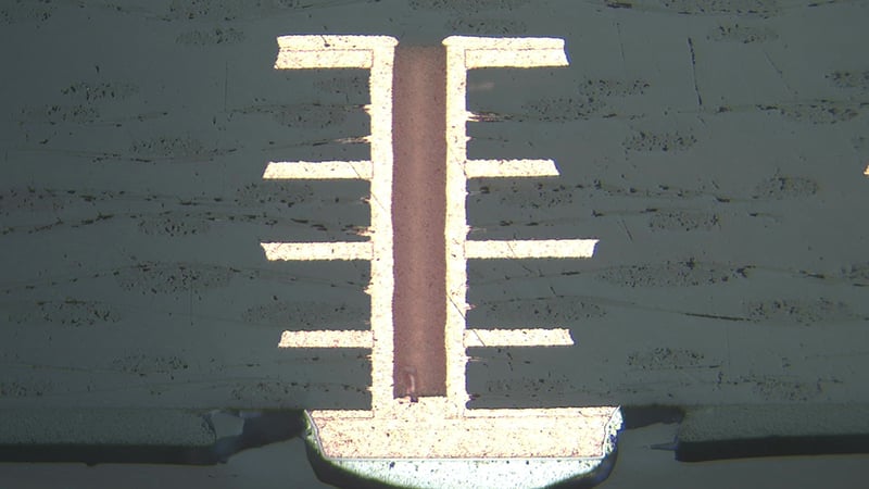
Example of bad wrap plating.
Summary
Copper wrap plating is a critical process in the manufacturing of printed circuit boards. It ensures that electrical signals can flow freely between layers of the PCB, improving signal integrity and overall reliability. Achieving high-quality copper wrap plating requires careful control of plating conditions, including the composition and concentration of the electroplating solution, the temperature and pH of the solution, and the current density applied to the board.
By carefully controlling these factors, manufacturers can produce PCBs with consistent and reliable copper wrap plating, ensuring that the finished product performs as intended.
Key Takeaways
- Wrap Plating Enables Reliable Layer Connections: Wrap plating is essential for creating continuous electrical paths through vias and through-holes, ensuring dependable interlayer connectivity in multi-layer PCB designs.
- IPC-6012B Specifies Strict Requirements: Industry standards mandate that wrap plating for via-in-pad structures must extend at least 0.025mm (1 mil) up the sidewall and be free of voids or thin spots to maintain electrical integrity.
- Electroplating Is the Core Process: Wrap plating is achieved using electroplating, which deposits copper onto drilled hole walls. Key process parameters, like solution concentration, temperature, pH, and current density, must be tightly controlled.
- Pulse Electroplating Improves Coverage: To ensure full copper coverage in small or complex holes, Epec uses pulse electroplating, which agitates the plating solution more effectively than continuous flow methods.
- Copper Thickness Must Be Balanced: A typical wrap plating thickness of 25–30 microns offer a solid conductive path without interfering with later manufacturing stages, striking a balance between performance and process compatibility.


