


In the realm of high-speed electronic design, controlled impedance is an absolute requirement for flex and rigid-flex printed circuit board (PCB) configurations. This blog post delves into the intricacies of achieving controlled impedance in these designs, examining the factors that influence it, the different configurations available, and their impact on PCB thickness and flexibility.
Controlled Impedance: A Prerequisite for High-Speed Signals
Controlled impedance is crucial for high-speed signal integrity. In flex and rigid-flex designs, achieving this typically requires a thicker core than standard, influenced by the dielectric constant of the materials and the required spacing between the signal layer and the reference plane. While a standard core might be 1 mil in thickness, controlled impedance often necessitates a minimum of 2 to 4 mils. This adjustment is vital for achieving the required controlled impedance but comes with a drawback in the increased overall thickness.
Advanced Impedance Requirements
For higher-end controlled impedances, such as 120-ohm differentials and 60-ohm single signals, even thicker cores are necessary. This is a direct consequence of needing to maintain specific impedance values while accommodating the physical constraints of the PCB materials and design. So, why are thicker cores needed for advanced impedance?

Maintaining Specific Impedance Values
The impedance of a PCB trace is influenced by its width, the dielectric material's properties, and the distance to the reference plane. Higher impedance specifications often necessitate thinner trace widths and or increased spacing between the trace and reference plane layers. This, in turn, requires thicker cores to accommodate these adjustments while preserving signal integrity.
Mitigating Signal Crosstalk and Attenuation
As signal speeds increase, the risk of crosstalk and signal attenuation also rises. Thicker cores provide more room to separate traces, reducing the likelihood of interference between high-speed signals. This separation is crucial in maintaining the clarity and integrity of each signal, especially in densely packed PCB layouts.
Dielectric Material Considerations
The choice of dielectric material plays a pivotal role in controlling impedance. Materials with a lower dielectric constant can allow for thinner cores. Selecting the right material is a balancing act between achieving the desired impedance and meeting the mechanical bend requirements of the application.
Design Strategies for Advanced Impedance Requirements
For stack-up optimization, designers must carefully plan the PCB stack-up to achieve the required impedance levels. This involves selecting the appropriate number of layers, determining their arrangement, and choosing the right core and prepreg materials. Simulation tools are often used to model different stack-up configurations and assess their impact on impedance.
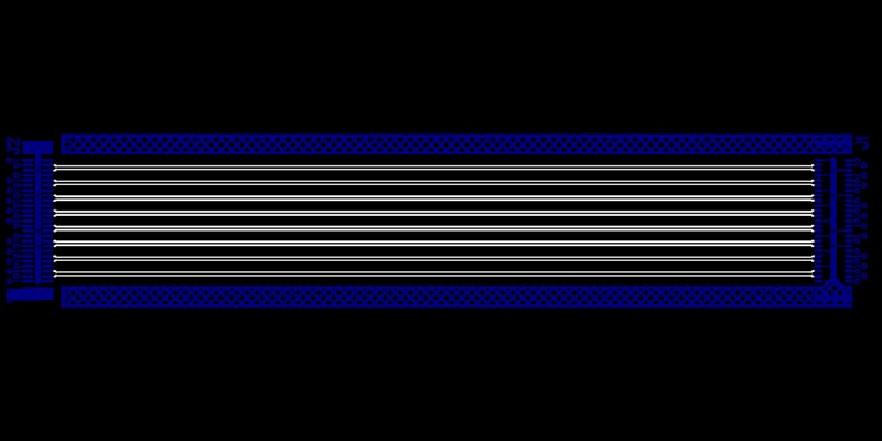
An example of a signal layer of an impedance design. The white lines are the highlighted impedance lines in the layer.
For trace geometry and routing techniques, advanced impedance requirements may necessitate specific trace geometries, such as thinner trace widths or differential pairs with precise spacing. Routing techniques also play a role, as the path and length of the traces can affect impedance. Designers must consider these factors in the context of the available space and the overall complexity of the PCB.
When it comes to prototyping, given the complexity and precision required for high-end impedance control, prototyping, and iterative testing are often necessary. This allows designers to validate their design choices, assess performance under real-world conditions, and adjust as needed before final production.
PCB Configurations for Controlled Impedance
Surface Microstrip
This configuration consists of two layers: one for signals and another acting as a solid ground reference plane. It's a standard approach for common impedance requirements like 100-ohm differential and 50-ohm single-ended signals.
Stripline Configuration:
A more complex setup, the stripline configuration sandwiches the signal layer between two reference planes. This offers full shielding of signal traces, crucial for meeting EMI and RF requirements. However, it increases the PCB thickness by about 60-67%, mainly due to the addition of the second reference plane and slightly thicker cores.
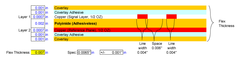
Stack-up example of a 100-ohm surface micro-strip differential pair.
Addressing EMI & RF Shielding
For shielding options, let’s look at EMI shielding films. These are preferred when impedance control isn't a priority, but when signal ‘noise’ is a concern. These films are laminated to the external surface, providing effective shielding without significantly increasing thickness. As an alternative, copper shield layers will be necessary when controlled impedance is a requirement. This option increases PCB thickness by about 50% but is essential for those impedance-controlled designs. A third option of silver ink shield layers is an older technology, and it is not recommended for controlled impedance applications.
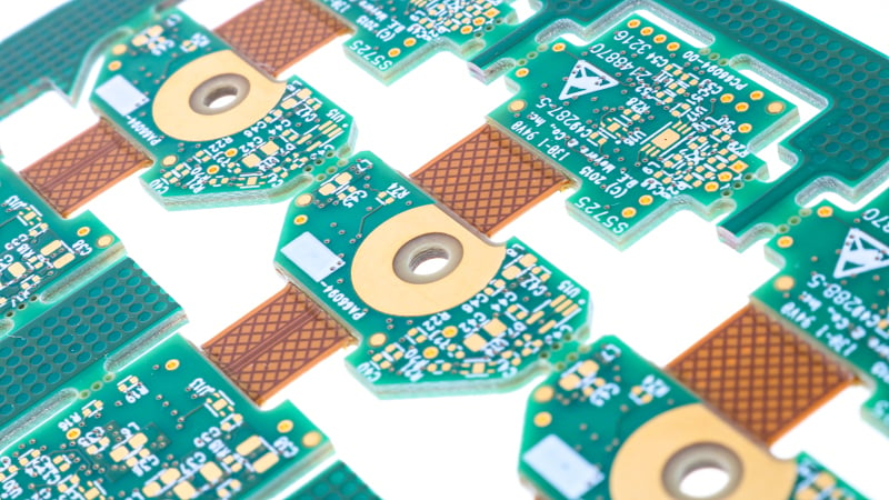
Example of a rigid-flex circuit board with shielding.
Current Carrying Requirements
In some PCB designs, addressing current carrying requirements when combined with controlled impedance is an aspect that significantly impacts the overall configuration of the board. When the design needs to accommodate higher current levels, the use of thicker copper becomes essential. This is particularly evident in designs where space is limited, and the option to use wider traces for increased current capacity is not feasible. As a result, the copper layers need to be thickened to handle the increased current without compromising the board's integrity or performance.
The incorporation of thicker copper layers will also directly influence the requirements for the adhesive layers used in multilayer PCBs. These adhesive layers play a crucial role in ensuring that the copper traces are securely bonded to the board and properly insulated. To achieve effective encapsulation and adhere to industry standards such as those set by the IPC (Institute for Printed Circuits), the thickness of the adhesive layer needs to be proportionate to the copper layer's thickness. Typically, the guideline is to use 1 mil of adhesive for every ounce of copper thickness. This ratio is critical to maintain structural integrity and avoid issues like delamination or electrical shorts, which can arise from inadequate bonding.
Design Complexity and Layer Count
As the complexity of a PCB design escalates, often driven by the need to incorporate more functionality into increasingly compact spaces, the solution frequently lies in adding more layers to the board. This escalation in layer count is a direct response to the challenge of accommodating a higher density of circuits and components within a confined area. Each additional layer, while providing more real estate for circuitry, also contributes to an overall increase in the thickness of the flex circuit. For instance, moving from a two-layer to a three-layer construction can lead to a substantial increase in thickness, sometimes by as much as 40%.
This increase in thickness, while necessary for meeting design complexity, can have implications on the flexibility of the circuit and its suitability for certain applications. Designers must carefully balance the need for additional layers with the inherent flexibility characteristics required for the end application. In some cases, advanced materials and innovative layering techniques may be employed to mitigate the impact on thickness, allowing for complex designs to maintain a degree of flexibility suitable for dynamic or space-constrained environments.
Summary
Controlled impedance in flex and rigid-flex PCB designs is a balancing act between maintaining signal integrity and managing physical constraints such as thickness and flexibility. The choice of configuration, materials, and layer count all play crucial roles in achieving the desired electrical performance while adhering to space and flexibility requirements. Understanding these aspects is key to successful PCB design in high-speed applications.
Key Takeaways
- Controlled Impedance Requires Thicker Cores and Strategic Stack-Ups: Achieving consistent impedance, especially for 60-ohm single-ended or 120-ohm differential signals, often requires thicker core materials (2–4 mils or more), which increases the overall thickness of the PCB, especially important in high-speed or RF applications.
- Trace Geometry and Dielectric Selection Are Crucial: Impedance is affected by trace width, spacing, and the dielectric constant of the materials used. Thinner cores or low-Dk materials can help reduce thickness while maintaining required impedance values.
- PCB Configuration Impacts Shielding and Signal Integrity: Surface microstrip is common for simple impedance needs, while stripline configurations offer better EMI shielding at the cost of increased thickness. For designs with EMI concerns but no impedance control, shielding films are preferred over copper or silver ink layers.
- Current-Carrying Demands Affect Copper and Adhesive Thickness: Boards that must handle both controlled impedance and higher currents need thicker copper layers. This, in turn, requires proportional adhesive thickness (typically 1 mil of adhesive per ounce of copper) to avoid delamination or electrical issues.
- More Layers = Less Flexibility and More Thickness: As circuit complexity increases, layer counts often go up. This can increase the overall thickness by 40% or more, potentially impacting flexibility. Designers must balance complexity, flexibility, and space constraints when planning high-speed flex or rigid-flex designs.


