


As with many of today’s high-speed rigid circuit board designs, flex and rigid-flex PCB designs also require controlled impedance signals. The impedance vales are the same, typically ranging from 50 ohm single ended up to 120 ohm differential pairs. However, there are differences in how the impedance values are achieved due to the mechanical bend requirements that a flex or rigid-flex circuit board must meet that a rigid PCB does not.
In this blog post we will cover a range of elements that are impacted by a controlled impedance requirement and strategies that will help lessen the impact on the mechanical bend capabilities of the design.

Flexible PCB Materials
The primary material used for both flex core layers, and the external Coverlay layers is Polyimide. As a material Polyimide is very well suited for achieving controlled impedance signal lines. It is a uniform and homogenous material with an improved DK value in the 3.2 to 3.4 range. The lack of a glass reinforcement eliminates the DK variations created by the glass weave and knuckles in the glass weave as seen in rigid PCB materials. Polyimide is also extremely uniform in its thickness due to its “cast” manufacturing process and that the layers typically range in thickness from ½ to 4 mils.
Polyimide flex cores are available with either Electro-deposited or Rolled Annealed copper. The type used is driven by the min. bend requirement necessary for the design and whether it is a “bend once to fit” or a “dynamic bend” application. The most common copper thickness used is ½ OZ copper. This allows for best combination of the thinnest possible construction with the tightest minimum bend capability and the highest degree of flexibility while still allowing for a reasonable degree of current carrying capability that will meet most design requirements. One potential item, for very high-speed designs, is that as of this time “smooth”surface coppers are not yet available which may create an issue with “skin effect”.
Polyimide cores are also available in two formats that differ in how the copper is attached to the Polyimide. The original material uses a layer of flexible adhesive, either acrylic or epoxy based, to glue the copper to the polyimide. The modern material has the polyimide cast onto the copper without using any adhesive and is referred to as “Adhesiveless”. While impedance controlled designs are possible with either material the preferred is the Adhesiveless. It eliminates the use on an additional material, the adhesive, with a differing DK value and generally allows for thinner more flexible constructions.
Controlled Impedance Configurations
The four primary layer configurations used to achieve controlled impedance in flex circuits are similar to those used in rigid PCB designs:
Embedded Microstrip
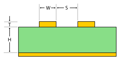
Edge Coupled Embedded Microstrip
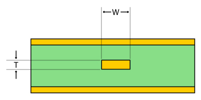
Symmetrical Stripline
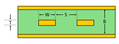
Edge Coupled Stripline
When applied to a flex circuit design the significant difference between the Microstrip and Stripline configurations, beyond the lack of shielding on one side for the Microstrip configurations, is the impact on the flex thickness and in turn the mechanical bend capability and reliability of the circuit.
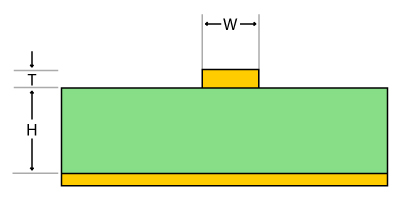
For maximum bend capability the 2-layer Microstrip is the preferred configuration. When combined with ½ OZ copper, a 0.002” flex core and 0.0005” Coverlays, the finished flex thickness is approximately 0.006” after lamination. This equates to a 0.060” min. bend radius using the general 10X thickness rule.
The Stripline configurations, while provided shielding on both sides of the circuitry, significantly increase the flex thickness and limit the bend capabilities of the part. In addition to the added shield layer and its associated dielectric core layer, both cores need to increase in thickness from 0.002” to 0.003”. For a design utilizing ½ OZ copper the finished flex thickness increases to over 0.011” after lamination. This limits the bend capabilities to over 0.200”.
The key element for both configurations is the use of ½ OZ copper. This allows for the sub 0.005” line widths necessary to achieve the impedance values when combined with the core thicknesses listed above. If 1 OZ copper is used the lines widths need to increase to 0.005” or greater due to etching process limitations. In conjunction the core thicknesses would increase to 0.004”. 1 OZ copper impedance lines increase the Microstrip version to almost 0.009” and the Stripline to almost 0.016”. The need for 1OZ copper is commonly driven by designs that have both impedance and higher currents. We recommend a careful design review to determine the available options which will meet the bend requirements.
Flex to Rigid Impedance Transitions
A unique element of a rigid-flex PCB design with controlled impedance is the need to change the configuration of the impedance lines as the circuits transition from the flex area(s) to the rigid area(s). It’s a common occurrence, in higher layer count designs, to have the flex areas impedance lines configured as a Microstrip but then, due to the need for power and ground planes in the rigid areas, have the configuration change to a Stripline. The preferred scenario is to maintain the same line width / spacing in both the flex and rigid areas by increasing the core thickness in the rigid area to the adjacent plane, but higher layer counts may not allow for the added thickness. The solution is to vary the line width and or spacing as the circuits transition from flex area to rigid area. This situation does not apply to Stripline configurations as the flex area reference planes extend throughout the rigid areas.
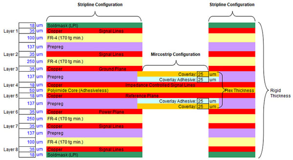
Example of an 8-layer rigid-flex circuit board construction.
Controlled Impedance and Higher Currents
The combination of both impedance control and higher current carrying requirements can create a design challenge. The thicker copper, for the current requirements, compounds with the impedance requirements to create an overlay thick flex construction that may not reliably meet the specified bend requirements. The solution is frequently unique for the specific design and may involve some of the following methods:
- Divorce current lines to separate flex layers in an Air – Gap multilayer flex construction
- Increase flex width to allow wider current lines with ½ OZ copper
- Utilize ganged current lines on multiple flex layers
- Restrict reference plane(s) to areas only directly above and or below impedance lines and utilize additional free space for ganged current lines
- Other options, TBD
The goal is always to minimize the flex thickness to the greatest degree possible in order to meet the bend requirements reliably.

Summary
Implementing controlled impedance in a flexible circuit or rigid-flex PCB design has additional considerations due to the mechanical bend requirements of the part. Controlled impedance, by necessity, increase the flex thickness. When combined with higher current carrying requirements it can further increase the flex thickness to the point where the bend requirements cannot be achieved. These challenges can be addressed in most designs with a complete design review and input from an experienced supplier.
Please feel free to contact Epec if you have any questions regarding the design of flex PCB with controlled impedance.
Key Takeaways
- Polyimide advantages in flex: Flex circuits use polyimide, which offers uniform dielectric properties, no glass weave distortion, and consistent thickness, making it well-suited for impedance control compared to rigid FR4 materials.
- Adhesiveless materials preferred: Adhesiveless polyimide eliminates adhesives with differing dielectric constants, enabling thinner, more flexible designs and improved impedance accuracy.
- Configuration impacts bend radius: Microstrip structures allow thinner builds and tighter bends, while Stripline designs add thickness and limit bend capability, trading flexibility for shielding.
- Copper weight is critical: Using ½ oz copper enables sub-0.005” line widths for impedance control and maintains flexibility, whereas 1 oz copper requires wider lines and thicker cores, reducing bend performance.
- Rigid-flex transitions add complexity: Impedance-controlled lines often shift from Microstrip in flex areas to Stripline in rigid areas, requiring adjustments in line width, spacing, or core thickness to maintain performance.


