


Flexible circuits, like other electrical interconnects, are subject to either receiving or emitting electromagnetic (EM) and or radio frequency (RF) interference. For critical designs, if allowed to occur, the performance of the assembly, or that of other local assemblies, can be compromised to the point of becoming non-functional. The difference between EM and RF interference is the frequency of the “disturbance,” with RF being in the radio frequency range and EM being typically 500 MHZ and higher. There are many potential sources of both types of interference within an assembly.
Shielding Design Challenges
Flex circuit shielding creates multiple design challenges that require careful review to ensure a successful part number. All shielding methods increase both the flex circuit thickness and cost to varying degrees. The thickness increase is most often the critical issue. It can easily lead to not meeting the bend requirements. This creates a reliability/mechanical breakage concern. The added cost can be significant. Beyond the added cost of the shielding materials the design can increase in layer count (i.e. from a 1- or 2-layer to a 3- or 4-layer construction).
Shielding is often combined with other electrical requirements; the most common is controlled impedance. This further increases the flex thickness and compounds the challenge of meeting both the electrical and mechanical design requirements.
The flexible circuit industry has multiple solutions that can be applied, which will eliminate both the absorption and or radiation of interference noise.

Copper Layers
The traditional shielding option, also used in rigid PCB design, is the addition of external layers of copper, either as solid or cross hatched planes connected to ground, sandwiching the signal layer(s) between them. In addition, ground lines can be run around the perimeter of the part to “seal” the edges in very sensitive applications.
While it is a very effective shielding solution, it has the negative impact of both significantly increasing the thickness of the design and the part cost. The added thickness reduces the bend capability/flexibility of the design and potentially creates a breakage reliability concern when the flex circuit is bent into its required shape. A 3-layer copper shielded flex circuit can be more than 125% thicker than a 1-layer non-shielded version.
The added cost can be significant if the design only requires a single layer of circuitry to achieve the interconnect requirements. The design now becomes a minimum of a 3-layer construction. The cost is incurred by both the added layers of materials and the many added process steps required to create the multi-layer circuit.
Cross hatching the copper shield layers will improve the design’s flexibility, but not to a significant degree and potentially reduce the level of shielding.
An added negative element is the stitching vias interconnecting the external shields along the length of the flex. Vias in the flexible areas is not a preferred design practice. They act as both mechanical stress concentrators and reduce flexibility which may prevent the flex from bending naturally.
Copper layer shields do have the advantage of allowing for controlled impedance signals in high-speed designs.
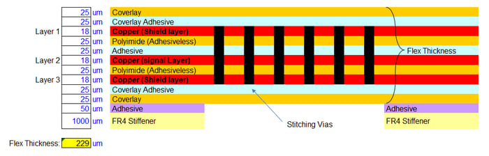
3-layer copper shielded flex PCB with stitched vias.
Silver Ink Shield Layers
An alternative traditional solution is silver ink shield layers. Silver ink has the advantage of both improved flexibility and reduced cost compared to copper layers. The ink is a more flexible material than copper but does require additional coverlay layer(s) to encapsulate and protect the silver ink. The result is still a thinner and less costly solution than that with copper layers. The level of shielding is effective for most applications. A silver ink shielded flex circuit can be as little as 75% thicker than a 1-layer non-shielded version.
Rather than vias, silver ink uses selective openings in the primary coverlay, which encapsulates the circuitry, and drilled holes in the flex core to expose the ground circuit and allow for its electrical interconnect. The silver ink flows into these openings and bonds physically and electrically to the ground circuit(s).
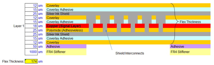
1-layer silver ink shielded flex PCB construction.
The lower cost of silver ink is primarily due to the design remaining as a 1-layer circuit. This reduces the number of material layers and manufacturing process steps required. The application of silver ink is a cost-effective silk-screening process.
Silver ink is not a viable solution for most controlled impedance designs.
Shielding Films
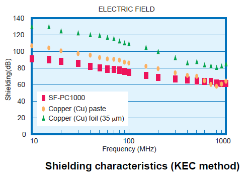
The most recent solution is specialized shielding films. These materials were specifically designed to meet the shielding requirements of flexible circuits. They allow for the thinnest possible constructions and are suitable for dynamic bend applications.
Shielding films are highly effective and have proven successful in many sensitive designs.
With the cost now being comparable to silver ink in most applications, the use of ink has diminished significantly and may no longer be supported by many flex circuit manufacturers. Unless the part number is an older qualified design, many designs can be easily converted from silver ink to shield films.
The material is supplied as a laminated 3-layer structure: an electrically conductive adhesive, a metallic deposition layer, and an external insulation layer. It is then laminated under heat and pressure onto the surface of the flex circuit coverlay and/or flex core and do not require any additional coverlay layers. They also have the added benefit of a slip property in the insolation layer to prevent the circuit from galling if abraded.
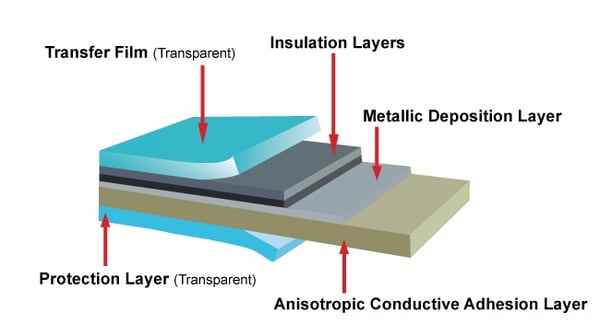
Example of cross section structure of EMI shielding film.
The interconnect method to the ground circuit(s) is the same as silver ink. Selective openings in the coverlay(s) allow the conductive adhesive to bond and electrically interconnect.
The impact on thickness is the least of the three options. A 2-sided shielded film design is only 15-20% thicker than the 1-layer non-shielded construction.
Shield films are not a viable solution for most controlled impedance designs.
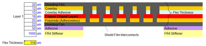
1-layer shield film shielded flex PCB construction.

Summary
Shielding requirements are a critical design element of flexible printed circuit boards. As with other electrical requirements, it requires a careful review of all the electrical and mechanical design parameters to ensure a functional, reliable, and cost-effective part.
Key Takeaways
- Shielding adds cost and thickness: All shielding methods increase circuit thickness and expense, which can impact bend requirements and overall reliability.
- Copper layers provide the strongest shielding: Solid or crosshatched copper planes are highly effective and support controlled impedance, but they add significant thickness, reduce flexibility, and require more processing steps.
- Silver ink offers balance of cost and flexibility: It delivers effective shielding at a lower cost and thinner profile than copper, but it is not suitable for most controlled impedance applications.
- Shielding films are the thinnest option: Designed specifically for flexible circuits, films provide excellent shielding with minimal thickness impact, making them ideal for dynamic bend applications.
- Ground interconnection methods vary by approach: Copper shields often require stitching vias, while silver ink and shielding films use selective openings to bond with ground circuits, preserving flexibility.


