


Etch compensation adjusts copper trace widths in printed circuit board (PCB) design data to offset material loss during the etching process. Without it, manufactured traces can fall outside tolerance, impacting reliability and performance. Proper use balances dimensional accuracy with spacing constraints, especially in high-density or heavy copper designs.
Etch compensation is the intentional adjustment of trace widths in PCB design data to account for dimensional changes that occur during copper etching. As unwanted copper is removed, trace features can shrink due to process variables such as copper thickness, etching quality, and the chemical properties of the etchant.
To maintain the intended geometry, PCB designers or CAM engineers increase the size of features in the artwork. This ensures that after etching, the remaining copper aligns with the original design intent and stays within specified tolerances.
The amount of compensation required varies based on manufacturing conditions and design requirements, making it a process that must be tailored for each application.
Why Etch Compensation Matters
Without adequate compensation, fine features can become too narrow or inconsistent, leading to failures in quality control or degraded electrical performance.
Key benefits of applying etch compensation include:
- Improved accuracy: Final trace widths more closely match design intent
- Better performance: Maintains signal integrity and reduces risk of distortion
- Reduced rework: Fewer post-production corrections or scrap issues
- Faster production: More consistent builds support shorter lead times
- Greater design flexibility: Enables use of different processes without sacrificing reliability
Ensuring proper compensation early in the design-to-manufacturing process helps avoid downstream issues.

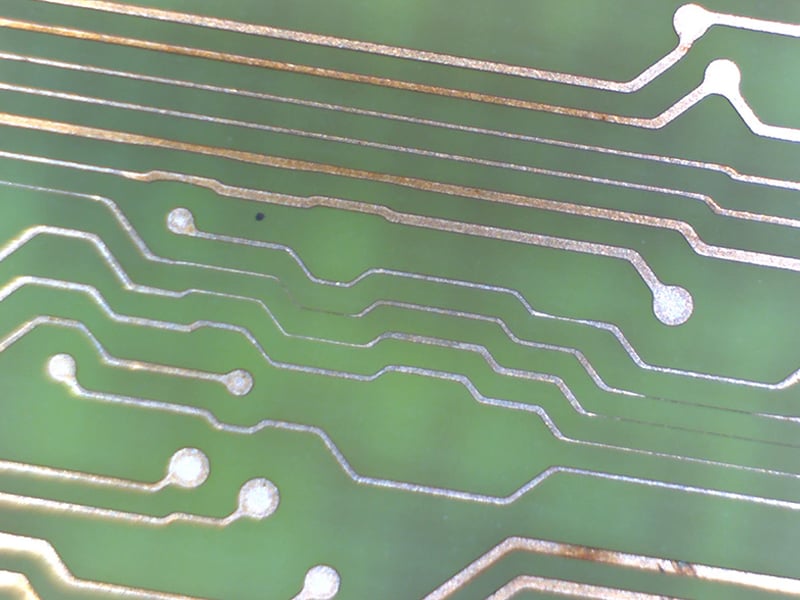
Example of a tight trace. This is what happens when there is no room to space out features and we opt NOT to etch comp them fully. Those thin dark traces are too small to be reliable and did not pass quality control.
How the Etch Compensation Process Works
During fabrication, PCB layers are patterned using photoresist and then etched to remove unwanted copper. Even with protective dry film, some of the intended copper features are reduced during this step.
To counteract this:
- CAM increases the surface area of the photoresist features in the artwork
- This anticipates copper loss during exposure to the etching solution
- The final etched traces “shrink” into the intended dimensions
This process is guided by empirical data and established rulesets to consistently meet tolerance requirements across different builds.
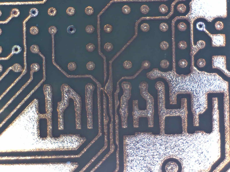
Illustration of what happens when we etch comp customer data BUT don’t have any room to space features apart.
Copper Loss, Trace Spacing, and Design Constraints
Etch compensation is not without tradeoffs. Increasing feature size before etching can create unintended spacing challenges, particularly in dense layouts.
Tight Trace/Space Designs
- When trace spacing is already minimal, compensation can cause features to overlap
- Overlapping features do not etch correctly and can result in defects or electrical issues
- Limited board real estate makes it difficult to resolve spacing conflicts after design
Higher Copper Weight Impact
Copper thickness directly affects how aggressively material is removed during etching.
- Thicker copper (such as 2oz) requires more etch compensation
- Increased compensation raises the likelihood of spacing violations
- Mixed copper weights across layers add complexity to compensation strategy
Designs with higher copper weights must account for this added variability early in layout.
Tradeoffs and Manufacturing Considerations
Applying etch compensation introduces a balance between dimensional accuracy and layout feasibility.
- Greater compensation improves tolerance control but increases spacing risk
- Tight layouts reduce flexibility for CAM adjustments
- Multilayer designs with varying copper weights require careful coordination
Even with precise rules developed through empirical data, risk remains when compensation forces feature adjustments in already constrained areas. CAM intervention to resolve spacing issues can introduce additional complexity, particularly when traces are closely packed or near drilled features.
Collaboration with CAM and Manufacturing
Successful implementation of etch compensation depends on coordination between design and manufacturing teams.
- PCB designers should understand compensation limits during layout
- Early engagement helps prevent spacing conflicts that require correction later
- CAM engineers use established rules to maintain tolerance while preserving functionality
Because PCB real estate is often fully utilized, proactive planning is critical to avoid conflicts that cannot be resolved without redesign.
Watch Recording Below:
Summary
Etch compensation is a critical step in ensuring that copper features on a PCB meet design specifications after fabrication. By adjusting trace widths to account for etching effects, manufacturers can maintain accuracy and performance, but this process must be carefully managed in tight layouts and designs with heavy copper.
Balancing compensation with available spacing, and collaborating early with CAM and manufacturing teams, helps prevent defects, reduces rework, and ensures consistent, reliable production outcomes.
Key Takeaways
- Etch compensation offsets copper loss during fabrication to maintain trace dimensions.
- Tight trace/space designs increase the risk of overlap when compensation is applied.
- Higher copper weights require greater compensation and careful planning.
- Accurate compensation improves quality, performance, and production efficiency.
- Early collaboration with manufacturing reduces risk and avoids post-design corrections.


