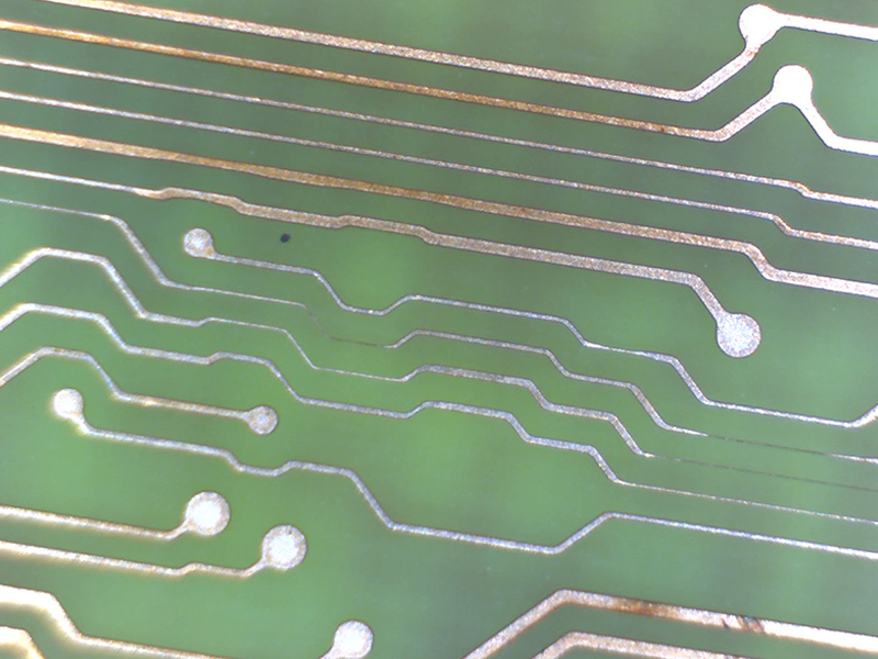
Etch compensation is a process used in the design of printed circuit boards (PCBs) to adjust the trace widths to compensate for any changes that occur during the PCB manufacturing process. When PCBs are manufactured, the etching process used to create the copper traces on the board can cause some amount of variation in the width of the traces. This variation can be caused by factors such as the thickness of the copper, the quality of the etching process, and the chemical composition of the etchant.
Read MoreNetVia Group

For more than 35 years, the most advanced and innovative technology companies have relied on NetVia Group for all their time-critical, high performance PCB solutions. In 2019, NetVia Group became a part of the Epec Engineered Technologies group of companies, which continue to hold true to the values of excellence that have driven NetVia since the beginning.


