


Devices are becoming smaller and thinner, requiring circuit boards that can fit into the equipment without adding any additional weight while being flexible enough to route around components. Flexible printed circuit boards offer high-density electrical connections while also reducing space.
Along the circuit board, flexible films and conductive materials are placed in layers. The number of layers used is dependent on the complexity of the design. To connect the electrical signal between the varying layers, a via hole is placed on the PCB.

Vias Holes in Flexible PCB Areas
Via holes, simply called vias, are holes that are used to make electrical connections between the layers of the design. Vias also come in a variety of shapes and types, such as through-hole, buried vias, blind vias, and microvias.
To create a via, a copper pad is placed at a specific location on each layer of the printed circuit board. The via hole is then drilled through the copper pad on each layer. Chemicals are used to dissolve any remaining epoxy and burrs in the holes as well as to expose the copper pads in the internal layers of the flex circuit. The flexible PCB then undergoes a plating process where a copper coating is chemically added into the holes in a process called electroless copper deposition before the entire board experiences a copper electroplating process and chemical bath cleanings. Lastly, etch resist is added onto the layers to define the circuit patterns the balance of the copper is chemically removed (etched).
Pros:
When it comes to using vias in flexible circuit boards, the main advantage is that they allow for higher complexity circuit routing. The vias route the circuitry through multiple layers throughout the design.
Cons:
If dealing with a device that requires complex circuit boards with multiple layers, manufacturers who must drill in vias may increase their production costs due to this potential complexity. Having a lot of vias also increase the potential of damaging the board during assembly, which may result in the need to scrap the flex circuit and create a new design. Depending on the placement of the vias, they can interfere with other nearby components and take up space that other components require depending on the number of vias that are used.
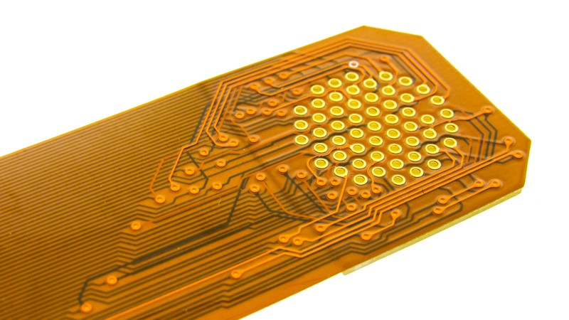
Example of a 2-layer flex circuit with vias.
Overview of Flexible PCB Areas
The flexible areas of the flex circuit are made up of polyimide substrates, adhesives, traces, and coverlays.
- Polyimide Substrate Film: Polyimide materials make up the dielectric substrate/core layer of the flexible part of the circuit board. This material forms the base where all the traces, vias, and other components are attached. Polyimide is the preferred material due to its flexibility, resilience, temperature resistance, and dielectric properties.
- Traces: The traces are the copper electrical conductors on the PCB that allow the signals to move along the circuits. For multi-layer flexible circuit boards, the traces are on multiple layers and staggered in relation to each layer if possible. The widest possible trace is desired and should be covered to allow the flex circuit to bend. This feature ensures the longevity and performance of the circuit board. In addition, rolled annealed copper is preferred over electro-deposited copper for its improved ductility.
- Adhesive Materials: Adhesive materials are used to join all the individual layers of the PCB together. The types of adhesive materials used are either flexible epoxy resin or acrylic based.
- Coverlay/Cover Coat: Coverlay is used as the external protective covering on the flex circuit. This coverlay, polyimide, is used in place of solder mask as it offers greater flexibility to this area while offering protection to the copper structures.
- Solder Mask: Solder mask is a photo-imaged liquid epoxy that can be applied to the bottom and top of the FPCB. It protects the copper from exposure and oxidation. The difference between solder mask and coverlay is that solder mask is liquid-based, and the coverlay is a solid polyimide layer with an adhesive.
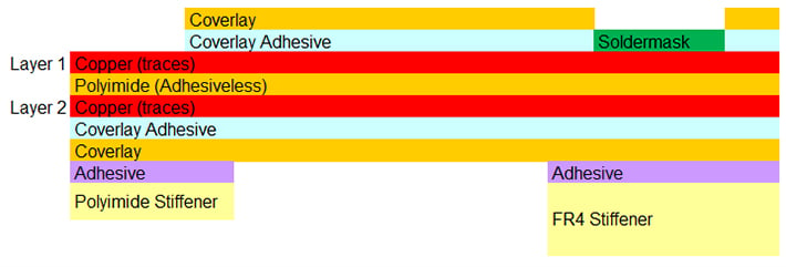
Example of flex PCB circuit material stack-up.
Benefits and Drawbacks of Using Vias
There are several benefits and drawbacks to using vias on flexible circuit boards. One of the additional advantages is that vias can be used to control the temperature within the circuit board. They allow heat from components to pass through the via holes to a heat-dissipating plane layer located below.
A drawback is that a via placed in a bendable area can be prone to cracking and should never be placed near the interface of a rigid area. The structural stability of the circuit board can be compromised when too many vias are added. Below we will dive into more about the types of vias available, the design considerations, and the pros and cons of using them for printed circuit boards.
Types of Vias
- Through-hole/Thru-hole: The term via and through-hole are sometimes used interchangeably. However, a through-hole is a via that goes all the way through the layers of the printed circuit board to the other side.
- Buried Via: A buried via is an internal via. It does not meet to an external layer of the surface of the board and instead connects internal layers. Example: via that connects only layers 2 and 3 in a 4-layer design.
- Blind Via: A blind via only goes partway through the board as it starts at the external layer. Example: via connects only Layers 2 and 3 in a 4-layer design.
- Microvias: A microvia is a via with a diameter of less than 0.006 inches. Unlike the other vias that are made with a mechanical drill, microvias are drilled using a laser.
Design Considerations for Vias in Flexible Areas
Flexible circuit boards can go through large amounts of mechanical stress due to their bending and flexing. Traces and via placed in these bendable sections can experience damage over time that cracks the electrical signal traces along the circuit board. Here are several design considerations to be aware of when selecting a flexible printed circuit board.
Location
Location is important so that the vias are not subjected to damage. Vias should not be placed in a bend area if possible. They should be within areas supported by mechanical stiffeners. A via also cannot be located on the edge of a stiffener as it may crack the via plating during the stiffener lamination process. Place vias at least 20 mils from any stiffener edge and 50 mils from rigid to flex interfaces.
Pad Size
Pad plating is designed to meet the mechanical bend requirements for flexible circuits. This method limits the thickness of the finished copper which improves flexibility, mechanical bend reliability, and improves controlled impedance signal performance. Typical design requirements for pad plated via pads are that the pad size should be a minimum of 0.010” larger in diameter in relation to the size of the via holes and through-holes.
Vias in Flexible Areas
If via in a flexed area are necessary, a minimum bend requirement review is required to ensure the reliability of the finished parts. The presence of vias in a flexed area will limit the minimum bend radius capability. Providing additional information such as bend radius, location of bends, and application use can ensure PCB reliability.
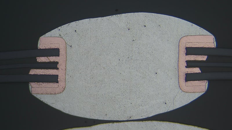
Cross section of via in flexible area.
Additional Manufacturing Considerations
While you may have set specifications that will need to be made for the flexible PCB to work with the application, the manufacturer that you partner with has design standards for you to be aware of based on their capabilities and the manufacturing equipment that is used.
Some of these design standards are the following:
- Vias in flex areas are not recommended by IPC 2223 design standard. IPC 2223 covers the standards for flexible PCBs, various component mountings, interconnection systems, and electrical constrain instructions.
- Vias in flexible areas can create mechanical stress concentrators that when the flex circuit is bent can lead to potential breakage. This may crack the plating in via(s). If necessary, locate away from the bend area in flex.
- In a rigid-flex PCB design, flex area vias add cost due to additional drilling and plating processes (similar to a buried via configuration in a rigid PCB) required. These costs need to be factored in and if possible, it is recommended that they be avoided if the design allows.
- Shielded designs, with Faraday cage requirements, require vias in the flex area(s) which cannot be avoided without compromising the shield effectiveness.
Summary
When designing and manufacturing flexible printed circuit boards, you want to ensure high electrical signal reliability no matter the number of laminated layers. Vias are the only solution to connect between layers and achieve the circuit routing requirements. However, there are technical items to be aware of to avoid damaging the flex circuit and or increasing your material and production costs.
Here at Epec, we manufacture flexible and rigid-flex printed circuit boards for a very wide variety of applications. Please feel free contact us to discuss the details of your specific design.
Key Takeaways
- Vias Are Critical for Multi-Layer Flex PCB Designs: Vias (including through-hole, buried, blind, and microvias) are essential for electrically connecting layers in complex flexible PCBs. They allow signal routing through stacked circuit layers while maintaining compact design footprints.
- Vias Can Add Complexity and Cost: Adding vias, especially in flexible areas, increases production costs due to added drilling and plating processes. Poor via placement can also risk damage during manufacturing or use, potentially leading to scrapped assemblies.
- Proper Via Placement Is Crucial in Flex Areas: Vias should never be placed in bend zones or near rigid-flex transition areas to prevent mechanical stress and cracking. IPC 2223 guidelines recommend placing vias at least 20 mils from stiffener edges and 50 mils from rigid-flex interfaces.
- Material and Structural Design Affect Via Reliability: The use of pad plating, rolled annealed copper, and proper trace width enhances via performance in flexible areas. Pad sizes should be at least 0.010” larger than the via diameter to maintain electrical integrity and physical resilience.
- Some Applications Require Vias in Flex Areas: While generally avoided, vias in flexible areas are sometimes necessary, such as for shielded designs requiring Faraday cages. In these cases, minimum bend radius reviews and close collaboration with the manufacturer are essential to ensure reliability.


