


From powering everyday gadgets like smartphones and laptops to complex systems in medical devices and aerospace technology, printed circuit boards (PCBs) are fundamental to modern electronics. They are essentially the heart and soul of all the electronic gadgets and devices that we use in our daily lives. For those in the PCB industry or even casual tech enthusiasts, understanding the basic principles of printed circuit boards is invaluable.
This blog post aims to provide a deep dive into the subject, exploring its components, variations, design process, manufacturing, quality assurance, and future trends.
What is a PCB?
Think of a PCB as a physical canvas or road map for designing electronic circuits. It provides a stable and conductive pathway for electrical currents to flow across a layer from one net to another, passing through plated holes to internal layers or the opposing side, allowing various components to interact with one another. Although seemingly simple, the design and manufacturing of a PCB are complex processes involving intricate details and precise specifications.

Key Components
Substrate
The substrate is the backbone of a PCB, typically made from a fiberglass/resin material known as FR4. To begin with the process of manufacturing this multilevel laminate all aspects are considered. They come in a variety of “flavors”, thicknesses, and copper weights. It offers mechanical support, and specific electrical properties, such as dielectric constant, temperature decomposition, flammability resistance, arc resistance, and loss tangent, which impact circuit performance.
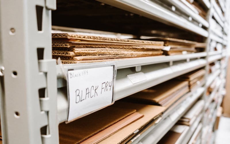
FR4 laminate material in storage.
Copper
The copper layer or layers are affixed to the substrate and etched to form the circuit traces. Copper is preferred due to its excellent electrical conductivity, but thickness and patterning must be considered when selecting materials for processing. The circuitry must be meticulously controlled through several strategic processes to maintain the desired functionality. Not all designs can be processed on all copper weights, consulting your PCB suppliers with stack-up advice is recommended in the early stages of design.
Copper Weight
- 5 oz/sq. ft: is commonly used for producing circuity <0.005” line width
- 1 oz/sq. ft: Standard for most applications
- 2 oz/sq. ft: Used in high-power or high-current circuits
Solder Mask
Applied over the copper layer, the solder mask insulates and protects the traces and is applied before the final surface finish. The mask layer prevents solder shorting and is critical for the ease of the assembly process. The mask protects the components by covering circuitry and or vias creating a barrier to keep the PCB from shorting during the wave soldering process.
Silkscreen
This informative layer is crucial during assembly and maintenance. It indicates component placements, their orientations, and other relevant data like test points, this road map is often overlooked as important and misunderstood as to what can and cannot be reproduced. The processing of legend is completed mostly as a screen-printed process and seldom as a digital print. The character height and draw width are critical to legibility. Unfortunately, the direction of PCBs, the technology, and the landmass available often do not allow for sizing requirements.
Types of PCBs
Single-Sided Circuit Boards
Most commonly used in simple electronics like calculators, time clocks, and alarms, the single-sided circuit boards have one layer of substrate and one layer of copper. They contain no plating and are simply a print-and-etch process to produce. Because of the simplicity of this type of PCB circuitry is usually of larger line width and fewer holes. Using only one layer of conductance can create a problem with space and routing the larger trace width can be challenging some of the time forcing the overall X/Y size of the part to increase.
Double-Sided Circuit Boards
Utilized in more complex circuits like computer motherboards, these boards have copper traces on both sides, which are connected by plated-through holes (PTHs). The processing time is increased with a 2-layer or double-sided PCB due to the addition of plating of the circuitry and holes. There are more processing steps for this type and double the available land for circuit routing and component placement. Many double-sided parts have components on the top side only using the bottom side to route additional traces needed to carry current.
Multi-Layer Circuit Boards
Employed in high-end applications like satellites and data servers, these boards consist of multiple layers of substrate and copper. They always have more than two layers, ranging up to 40 or more for extremely complex applications. The lamination process adds time and cost to this PCB, and the complexity of the part will also up the manufacturing cost.
Flexible and Rigid-Flex Circuit Boards
Flexible circuit boards are used in wearable electronics, while rigid-flex boards are often seen in high-reliability applications like aerospace and medical devices. There are different processing steps including manual labor to flex and rigid-flex PCBs as well as cost increases. The materials and processing are specialties, and not all manufacturing services can produce this product.
The Design Process
Schematic Capture
Initial concepts are drafted in a schematic diagram using specialized software like Altium or Eagle. This step is crucial for defining how the circuit components will interact.
Layout
After the schematic is finalized, designers use PCB layout software to arrange components and traces physically. Design rules and constraints, such as minimum trace width and clearance, must be followed.
Gerber File Generation
A Gerber file serves as the manufacturing blueprint for the PCB, including details like copper trace layout, hole locations, and component placement.
Manufacturing Steps
- Material Preparation: Substrate is cut to required dimensions.
- Copper Lamination: Copper foil is laminated onto the substrate using heat and adhesive.
- Imaging: Photoresist material is applied, and a circuit pattern is exposed to it.
- Etching: Exposed copper is removed, leaving behind the desired circuit traces.
- Drilling: Holes for through-hole components and vias are drilled.
- Solder Mask Application: Masking material is applied and cured.
- Silkscreen Printing: Essential information is printed onto the solder mask.
- Surface Finish: Final coating, usually HASL or ENIG, is applied.
- Assembly: Components are soldered onto the board.
Quality Assurance and Testing
Visual Inspection
A visual inspection is performed from the data level throughout production to the completion of the final PCB. Software programs are essential to accuracy but even thermal starvation or a small defect like a hairline crack can result in circuit failure. Visual and AOI (automated optical inspection) performance is key to quality product consistency and assurance or repeatability.
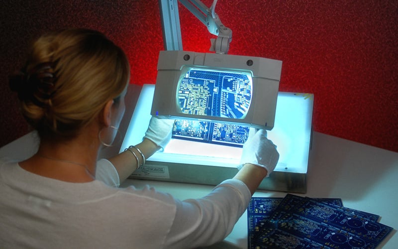
Visual inspection of PCBs under a microscope.
Electrical Testing
Using techniques like Flying Probe or Bed of Nails tests, each board is verified to function as intended electrically. Not all manufacturers certify 100% electrical testing of all PCBs knowing your testing promise from your supplier.
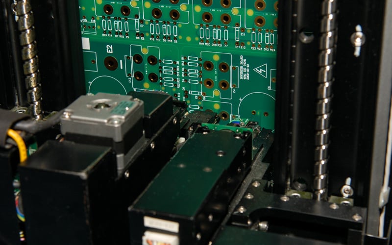
Flying probe electrical testing on a PCB.
X-ray Inspection
For multi-layer boards and complex assemblies, X-ray inspection may be conducted to check internal features. The critical registration of internal cores can only be checked using an X-ray without it the verification process is unknown. The material used for PCBs is prone to shrinkage and growth, the changes have become predictable, the processes have tightened up, and the X-ray gives peace of mind and confirmation that the process is dialed in.
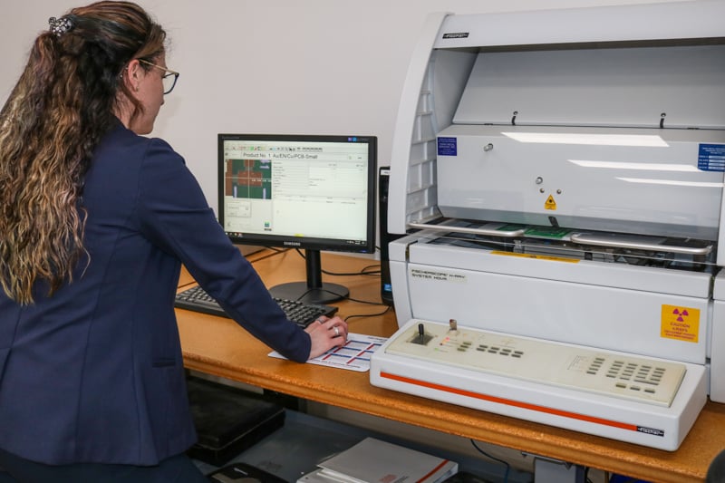
X-ray machine measuring materials used in PCBs.
Summary
Understanding the intricacies of PCBs is more than just a technical exercise; it's a doorway to grasping how our interconnected, electronic world functions at its core. From the foundational materials like the substrate and copper layers to the advanced design and manufacturing processes, each step is a testament to engineering precision and innovation.
Mastering the basics of printed circuit boards enables you to appreciate the challenges and opportunities that lie ahead in this ever-evolving field. Whether you are a seasoned engineer, a student aspiring to enter the industry, or a tech-savvy individual curious about the building blocks of your gadgets, delving deep into the world of PCBs offers invaluable insights. As technologies continue to advance, featuring miniaturization, high-speed data, and an increased focus on sustainability, the role of PCBs will only become more critical. This comprehensive guide aims to serve as a seminal resource, equipping you with the knowledge to understand, adapt, and excel in this dynamic landscape.
Key Takeaways
- PCBs are the foundational structure of modern electronics: Printed circuit boards serve as the physical and electrical platform for virtually all electronic devices, enabling complex component interaction across multiple layers.
- Each PCB layer and component serves a specific function: Elements like the substrate (FR4), copper layers, solder mask, and silkscreen work together to provide mechanical support, conductive pathways, insulation, and component labeling.
- There are several types of PCBs, each suited to specific applications: From single-sided boards in simple electronics to multi-layer and rigid-flex designs in aerospace and medical devices, PCB complexity scales with the device's performance requirements.
- Precision in design and manufacturing is critical to performance: The PCB design process involves schematic capture, layout, and Gerber file generation, followed by meticulous manufacturing and quality control steps like X-ray inspection and electrical testing.
- Mastering PCB fundamentals enables innovation in tech: Understanding the materials, construction methods, and testing processes behind PCBs empowers engineers, students, and hobbyists to innovate in an increasingly electronics-driven world.


