


In printed circuit board (PCB) designs, through holes are used to connect components and conductors on different layers of the board and can be divided into two types: plated and non-plated through holes.
Plated through holes are holes in the PCB that have a metal layer coating the inside of the hole, which is used to create electrical connections between different layers of the board. Plated through holes are typically used for components that require a reliable electrical connection, such as ICs (integrated circuits), connectors, and switches. Plated through holes can be created during the PCB manufacturing process using a chemical process called electroplating.
Non-plated through holes are holes in the PCB that do not have a metal coating on the inside of the hole. They are used to create connections between different layers of the board in a way that does not require a reliable electrical connection. Non-plated through holes are typically used for components that do not require a high degree of electrical reliability, such as passive components like resistors and capacitors. Non-plated through holes can be created using a mechanical drilling process during PCB manufacturing.
And I thought plating vs. non-plating PCBs is a short subject to discuss. On my initial approach to this topic, I thought, what could I possibly say about this that is worth putting on paper? Well, as I thought about it some more, I believe some clarity would be helpful.

Types of Printed Circuit Board Platting
When we discuss the plating of PCBs, it is more than just the circuitry surface. True, the traces and pads have a starting copper weight on the external layers. Most PCBs start with a ½oz or 1oz copper foil, others have more copper, 2oz, 3oz, etc. but the base copper is added, too. Internal layers are base copper only. An image is printed onto the film, polymerized by UV light, the nonsolid film is washed away, and the exposed copper is etched, leaving behind the circuit image. For the external layers, the film image supports non-circuit copper, the design, additional copper is added to the circuitry, pad surface, and holes. The polymerized film is stripped away, and the copper is removed and leaves behind the image. It’s complicated – with negative image, positive image, combined images – but still a very cool process.
Non-Plated Through Holes
Single-layer PCBs used to be bought by the thousands, stacks and stacks of them. A single-sided or 1-layer PCB actually contains no additional copper, hence no plating process. The laminate, FR4 material, is drilled, imaged, processed, and done. It is a little more complicated than that, but no plating is involved.
The holes in the laminate are drilled to the desired finished size; there is no plating in the holes or on the pad surface. The copper start weight is the finished weight. The critical item to know on single-sided circuit boards is the hole size needed because there is no plating involved those holes can be a standard +\-.002 tolerance drilled to size. The key to this is having the size needed. A 0.028” hole should be drilled 0.028”, giving the drill a 0.0005” tolerance in diameter using the +\-0.002” allows production to up or downsize with the available drill.
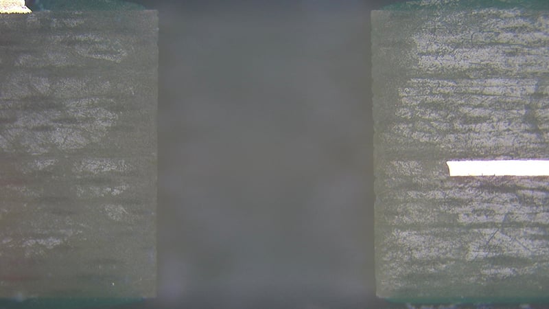
Example of a non-plated through hole.
Plated Through Holes
Now, plating is added to 2-layer PCBs and up, so it doesn’t matter how many additional layers are involved there is an addition to the copper weight. Typically, no plating is added to the internal image; the printing and the etching of copper are followed. The exception is buried vias. These holes will have plating and filling completed prior to the image. All holes that are plated transfer current from layer to layer.
Regarding signal, the signal transfer requires a connection through the holes. As a standard, any plated hole should have a tolerance of +\-0.003” with special considerations noted. Just as non-plated holes have a standard of +\-0.002”. The hole plating process is completed leaving a 0.0009 - 0.001” average thickness along the wall surface.
All plated holes are plated within the tolerance to allow the fit of the components using the tolerances provided. When a <0.003” +\- is provided, there will be a discussion on a change to an equal of 0.006” so +0.002”/-0.004”, or other.
When a deviation is not allowed, further pricing adjustments may be needed to meet the nonstandard tolerance. Surface plating of circuitry is also completed in conjunction with some of the hole plating. The image provided is initially printed onto the copper surface with additional plating applied to meet the final copper requirement. The circuitry is left as copper and protected by an application of solder mask. All remaining areas are then plated with the final surface finish coating. Coatings like, OSP, immersion silver, tin, and gold are applied as a final coating.
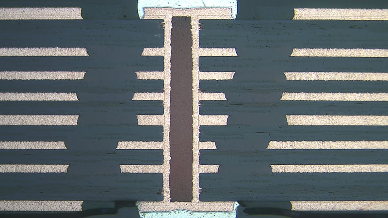
Example of a plated through hole and filled via.
Summary
The choice between plated and non-plated through holes depends on the specific requirements of the PCB design. Plated through holes are more expensive to manufacture than non-plated through holes but provide a more reliable electrical connection. Non-plated through holes are less expensive to manufacture but may not provide as reliable of an electrical connection as plated through holes.
And as you can see, several cycles of plating are applied to PCBs; the process is a longer loop for multiple-layer circuit boards with more complexity added as blind and buried or stacked vias are introduced. The plating is a critical component of the quality produced PCB. Your supplier should be monitoring this specialty process to ensure the quality standards of IPC are met. Items such as hole wall plating, surface plating, and final coating measurements should be available as part of standard paper workmanship. Knowing and trusting your PCB supplier to meet the standard should be an area you can trust when it comes to plating requirements.
Key Takeaways
- Plated through holes provide electrical connections between PCB layers: These holes have a metal coating inside to ensure reliable conductivity for components like ICs, connectors, and switches.
- Non-plated through holes do not have internal metal coatings: Used primarily for mechanical mounting or components that do not require electrical connections, these holes are simply drilled through the circuit board material.
- Plating processes impact PCB manufacturing complexity and cost: Plated holes require electroplating and additional processing, making them more expensive and time-consuming to produce than non-plated holes.
- Tolerances for plated and non-plated holes differ: Plated holes typically have a standard tolerance of ±0.003”, while non-plated holes generally have a tighter ±0.002” tolerance due to the absence of plating thickness variations.
- Proper monitoring of the plating process ensures PCB quality: A reliable PCB supplier should provide quality control documentation on plating thickness, hole wall integrity, and surface finish coatings to meet IPC standards.


