


In the realm of printed circuit board (PCB) engineering, the design incorporates through holes as a means to establish connections across the board's various layers or secure the card during the assembly process. These through holes come in two distinct categories: plated and non-plated.

Plated Verses Non-Plated Through Holes
Plated through holes in PCBs are essentially holes that feature a metallic coating along their interior. This coating facilitates electrical connectivity across the different PCB layers. They're most commonly employed for components demanding stable electrical connections, like integrated circuits (ICs), various connectors, and switches. The creation of plated through holes is typically achieved through a chemical method known as electroplating, incorporated during the manufacturing phase of the PCB.
Conversely, non-plated through holes in PCBs are characterized by the absence of a metallic lining within the holes. Their purpose is to enable layer-to-layer connections on the circuit board without necessitating robust electrical continuity. These types of through holes are often utilized for components where electrical reliability is not a paramount concern, such as passive elements like resistors and capacitors. They can also be used for securing large components to a PCB or securing the PCB during assembly or in the final unit. The process of forming non-plated through holes generally involves mechanical drilling, a step integrated into the PCB manufacturing workflow.
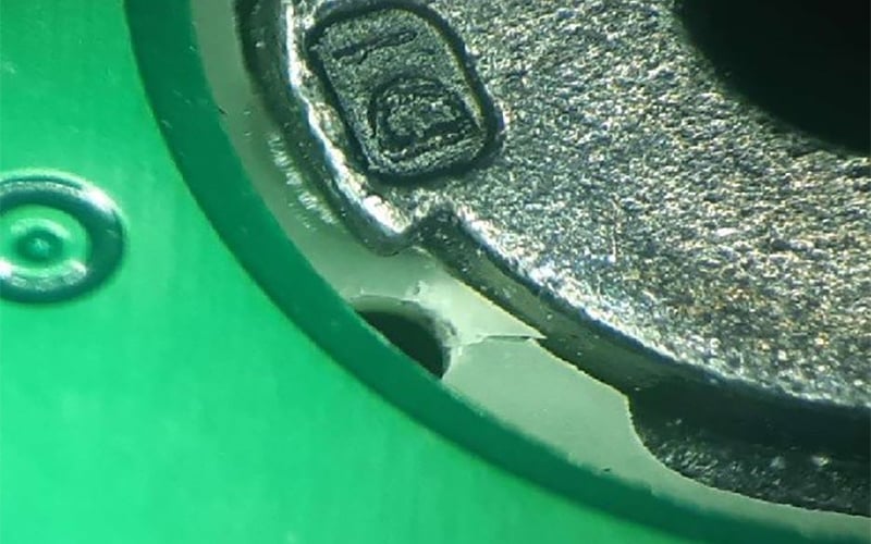
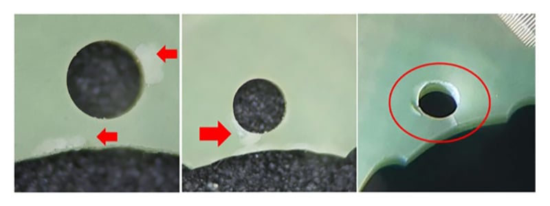
Fracturing of laminate material due to tight location of non-plated drill hole to board edge.
Single Sided Circuit Boards
In the past, single-layer PCBs were acquired in vast quantities, with countless stacks of them being purchased. These single-sided or 1-layer PCBs are distinct in that they lack any additional copper layer and, consequently, do not undergo a plating process. Their fabrication involves using an FR4 material laminate that is drilled, imaged, and processed, though this is a somewhat simplified description of the procedure.
For these PCBs, the holes are drilled to their final size right from the start. There's no plating within these holes or on the pad surface. The copper's initial weight is also its final weight. A crucial aspect of single-sided circuit boards is the precise size of the holes. Since no plating is used, these holes can be drilled with a standard tolerance of ±0.002 inches to the required size. The key here is accuracy in the hole size. For instance, a hole intended to be 0.028 inches should be drilled at exactly 0.028 inches, allowing for a 0.0005-inch tolerance in diameter. The ±0.002 inch tolerance provides flexibility in production, enabling adjustments in size based on the available drill bit.
In the intricate world of manufacturing small components, even the slightest deviation can lead to significant consequences. A fascinating instance of this is observed in the fracturing around non-plated holes in very small parts, typically just over ½ inch in diameter and merely 0.020” thick. These parts, due to their minute size and delicate nature, present a unique challenge in production.
Magnified Insights: The Phenomenon of Chattering
The issue at hand is often only visible under magnification. The fracturing observed around these non-plated holes is not immediately alarming since it doesn't compromise the spacing to copper conductors - a crucial aspect in manufacturing. Interestingly, there are no copper features near the affected areas.
This phenomenon is known in the drill rout world as "chattering." This occurs during the production process when a panel, containing hundreds of these small parts, progressively loses rigidity as more parts are drilled or routed out. This loss of rigidity can cause slight vibrations during the manufacturing process, leading to the observed chattering.
Fracturing of laminate due to “chattering” of drill bit during drilling or routing.
Customer-End Challenges: Press Fit and Rotation Stresses
At the customer's end, the real impact of this fracturing becomes evident. When these parts are assembled, they are press-fitted and rotated, actions that apply stress to the already fragile areas. This stress can cause the part to crack completely at the fracture points, leading to functional failures.
Identifying the Root Cause: Design Considerations
A closer examination reveals that the root cause of this issue lies in the design of the part itself. The non-plated drilled holes are positioned too close to the routed edge. This proximity doesn't leave enough laminate material to absorb the stresses of both the manufacturing process (drill/rout) and the customer's assembly process (press fit/rotate).
A Practical Solution: Redesigning for Resilience
To mitigate this issue, a redesign of the part is necessary. The non-plated holes need to be placed further away from the routed edge. This alteration would leave sufficient laminate material to effectively absorb the stresses encountered during both the production and assembly processes.
By addressing the design flaw, PCB manufacturers can significantly reduce the risk of part failure, ensuring a more reliable and robust component for their customers.
Single-sided, 0.031” thick PCB. The location of non-plated drill holes to board edge can lead to fracturing of laminate in the final assembly.
Summary
Understanding fracturing in non-plated holes illuminates the delicate balance required in PCB engineering, where minute details can have profound impacts. The contrast between plated and non-plated through holes in PCBs highlights the diverse needs and challenges in circuit board design and manufacturing. Plated holes, essential for components needing stable electrical connections, and non-plated holes, used for less critical connections, each play a vital role in the functionality and reliability of PCBs.
The phenomenon of 'chattering,' exemplifies how even the smallest manufacturing variance can lead to significant issues, such as part failure during customer-end assembly. This calls for a thoughtful redesign of parts to ensure robustness and reliability, considering factors like hole placement and stress absorption. Overall, this exploration into the intricacies of PCB manufacturing not only sheds light on the specific issue of fracturing in non-plated holes but also serves as a broader reminder of the critical nature of meticulous design, thorough process evaluation, and adaptive methodologies in the production of small, yet complex, components.
Key Takeaways
- Plated vs. Non-Plated Holes: Plated through holes provide electrical connectivity across PCB layers, while non-plated holes serve mechanical functions or low-reliability connections.
- Single-Sided PCBs: These boards don’t undergo plating, making hole size accuracy critical, with tolerances of ±0.002 inches playing a key role in performance.
- Chattering Effect: During drilling/routing of small, thin boards, loss of rigidity can cause vibrations that lead to laminate fracturing around non-plated holes.
- Customer-End Failures: Stress from press-fitting and rotating components in assembly can exploit these fractures, causing cracks and functional failure.
- Design Redesign is Key: Relocating non-plated holes further from the board edge leaves more laminate material to absorb stresses, improving durability and reliability.


