


As I think about the processing of multi-layered printed circuit boards (PCBs), I find it interesting that in the early 1980s, I wouldn’t have dreamed of where we are today in terms of technology. I mean, think about it. Where we are in comparison to then is simply phenomenal.
If nothing else, for example, the telephone in our homes. Remember how it was bolted to the wall with a never-ending entangled cord that limited where you could talk, and you can forget about privacy! Remember years later when we got call waiting or cordless? The dramatic time hop from the start of PCBs in the early 1900s to the present time has large spans of “not much has changed” to “wow” technology growth.
In this blog post, we will discuss how the unthinkable became a reality due largely to multi-layer circuit board technology.
What Is A Multi-Layer Circuit Board?
With anything electronic, there is some wiring involved, some process to make it work, and a PCB. If not for the printed circuit board technology none of what we have today would have been possible. In fact, the big thank you goes to multi-layered PCB hands down. So, what is a multi-layer PCB? Simply put, it is a PCB that has more than 2 layers to build, so 3 layers and up would be considered a multi-layered circuit board.
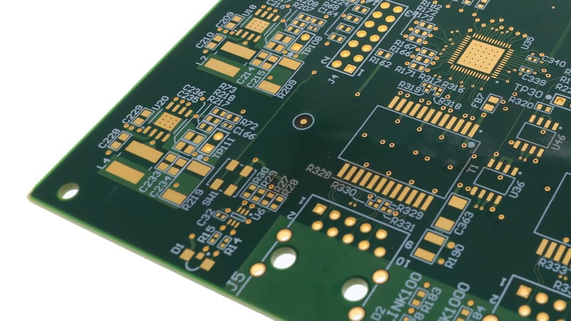
Example of a multi-layer circuit board.
A multi-layer PCB is essentially a sandwich of multiple layers of conductive copper traces and insulating substrate material. Each layer can have its own distinct circuitry, and they are interconnected using plated-through holes (PTH) or vias. The advantage of using multi-layer PCBs is the ability to increase the complexity and density of the circuits in a confined space. This technology allows engineers to design more compact, faster, and efficient electronics.
Mechanically speaking, multi-layer PCBs have the added benefit of increased structural rigidity, which is especially valuable when the circuit board size is large. From the perspective of electromagnetic compatibility (EMC), having multiple layers can also allow for dedicated ground and power planes, enhancing signal integrity and reducing noise interference.
In the PCB manufacturing process, each layer is etched separately and then bonded together under heat and pressure using a special adhesive. This ensures a strong mechanical bond and an excellent electrical connection. It's an intricate and precise process that demands a blend of mechanical engineering know-how with the finesse of electronics.
What Is A PCB Core?
Multi-layers consist of a core material in the center of the external layers. For ease of explanation of core processing, we are going to disregard ODD numbered PCBs like 3, 5, 7 layers and talk 4, 6, 8 layers instead.
What is a core? The core is a piece of substrate composed of woven glass, epoxy, and copper that is produced in many different thicknesses. Picture a thin piece of wood or other material with a thin layer of tin foil glued to the top and bottom. The copper bonded to both sides of the fibrous woven material is provided in large sheets that are cut down to size or in standard manufacturing panel sizes. The core is manufactured in many different thicknesses with different copper thicknesses applied to the material. The overall thickness is determined by the glass/epoxy and the ounce of copper applied to each side.
Once the desired number of layers is determined, these cores and prepregs are alternately stacked, ensuring that copper layers intended for circuitry face outward or interface with a neighboring prepreg. This stack-up is then subjected to a lamination process where heat and pressure are applied, causing the prepreg to flow, bond, and solidify, thus creating a singular cohesive multi-layered structure. The alignment of these layers is crucial, and mechanical precision is of utmost importance to ensure the vias (small holes) can connect circuits from one layer to another seamlessly.
The PCB materials are fire retardant and they do come in many other types of materials such as Teflon, ceramic, and aluminum. For the purpose of this blog post, we will discuss FR4 only throughout.
Multi-Layer PCB Stack-Ups
The multi-layer PCB is made up of cores with different thicknesses and prepreg material to bond the layers together, this is known as a stack-up. Layers of cores, prepreg, and copper foil in various thicknesses bonded together by heat and pressure to create the final PCB.

The stack-up is often suggested as layers, copper ounce, and final thickness leaving the dielectrics up to the printed circuit board manufacturer to determine cores. A balanced construction is often the go-to. A balanced construction is where the layers and prepreg are close to the same thickness. Unless impedance is part of the equations a balanced construction is advantageous to manufacturing and cost. Notoriously a core is a lesser cost than many sheets of prepreg to build a thickness.
Processing a Core
Cores are purchased at a specific thickness and copper weight. The material is precleaned prior to applying photo-imageable film to both sides. The film is then imaged with a circuitry design, developed to remove the non-circuitry film. The exposed copper is etched away leaving only the copper features behind. The core being an internal layer, for example, layer 2/3, is processed and completed. Production will repeat this process for as many internal cores as are needed to complete the part. If the core requires buried or blind holes, the process is then modified to drill and plate the holes, and the press and stack-up changes for the specialty process.
When the cores are completed, the next step is lamination. This step is completed when the copper foil has prepreg and cores added to the book or sandwich, alternating cores with prepreg until the final piece of copper foil is applied to the top side. The completed book is then baked under pressure until cured. Once removed from the press, the book is broken out of the plates, cleaned up, and sent to x-ray and drilling.
Time to Produce Lamination Cycles
The number of lamination cycles is totally dependent on technology, if there are blind or buried vias this adds lamination cycles to the process. The more sets of this type of via that there are the more lamination cycles the PCB will see. The average lamination cycle is 4-6 hours in length. Other items that can add to the length of process time are heavier copper thicknesses and layer counts. The thicknesses decrease the number of master panels per load, therefore increasing the number of loads required to complete the part. Time to process always adds cost to any manufacturing, labor, machine time, materials all of these increase cost.
Every buried or stacked via requires a lamination cycle.
Summary
Multi-layer PCB production is a complex process that hinges on numerous variables, from copper weight and circuit widths to the intricacies of dielectric construction. Factors such as the type of vias (blind, buried, or both), the balance of copper cores, and the chosen materials all influence the processing time and complexity.
The more complex a printed circuit board is, the more time it takes to complete the production process it needs. Copper weight vs. circuit widths, dielectric construction, blind, buried, or both types of vias, unbalanced copper cores, and even material type can play a factor in processing. Consulting with your PCB manufacturer for advice on stack-up materials and improved design ideas are always advantageous to cost and delivery. PCB manufacturing services with a knowledgeable staff of engineers like Epec are harder to come by domestically. At Epec, we offer free DFM, 24/7 engineering support as well as design and layout services.
Key Takeaways
- Multi-layer PCBs enable compact, complex designs: They combine multiple copper and substrate layers using cores, prepreg, and plated-through holes, offering increased density, better EMC performance, and enhanced mechanical strength.
- Core and stack-up design impacts cost and manufacturability: A balanced stack-up using fewer prepreg layers and more cores reduces cost, improves structural stability, and simplifies the lamination process.
- Lamination cycles are time-intensive: Each lamination cycle takes 4–6 hours, with extra cycles required for blind and buried vias, heavier copper weights, and higher layer counts, all of which increase time and cost.
- Processing precision is critical: Layer alignment, drilling, and via plating require mechanical accuracy to ensure seamless interconnections between layers, especially in high-layer-count boards.
- Early collaboration reduces lead times & costs: Working with experienced PCB manufacturers for stack-up recommendations, DFM reviews, and material selection helps optimize designs for cost, manufacturability, and delivery timelines.


