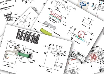
Prototyping is one of the most critical stages in the development of any electronic product. A well-designed printed circuit board (PCB) prototype can help you validate your concept, detect flaws early, and streamline the transition to production.
However, prototyping also brings a unique set of challenges that require careful consideration. Here are the key PCB design and production aspects you should pay attention to when creating a prototype.
Materials
Choose the right substrate material. In prototyping, the default choice is often FR-4 due to its lower cost and decent performance. However, for high-frequency applications or those with thermal demands, consider materials like Rogers, I-Speed from Isola, or Tachyon. Matching the substrate to your application avoids surprises in later testing stages.

Prototype PCB for a high-frequency application.
Your prototype should be built with materials matching the concept. Considering high-temperature materials for lead-free processing. Staying away from specific brand labels also increases the chance of going straight to manufacturing without delays.
DFM
While you may not be optimizing for mass production just yet, Design for Manufacturability (DFM) should still be on your radar. Avoid features that are difficult to manufacture (like extremely fine traces or tight vias) unless necessary.
Collaborating with Epec early on with your PCB design early can highlight any potential manufacturability issues before they become expensive mistakes. Our DFM service is always available and free! Real-life engineering correspondence and communication to aid in quick resolution and improvements to your current design. DFM can save time to market, cost for respin, and lost revenue.
Layer Count
Prototype boards often benefit from 2- or 4-layer designs for simplicity and cost. However, your application may require more layers for signal integrity or power distribution. Always plan your stack-up early and ensure signal layers are paired with ground planes to minimize EMI.
Considering additional layers as the first option instead of blind or buried vias will keep the cost lower and ease of manufacturing. Stack-ups can be tricky to manage in production when dielectrics are uncommon; note impedance values and allow for adjustments to be made by your supplier when it comes to stack-ups.
Footprint – Placement, Testing
Use verified footprints from trusted libraries or manufacturers to reduce the risk of misalignment or assembly issues. Considering space and trace in relation to components in early prototypes to allow easier manufacturing, they should match closely with the total board technology.
Maximizing land, allowing for the largest PCB size, will increase component placement options and possibly keep all assembly to one side of the circuit board.
Test Points and Debugging Features
Include accessible test points for power, ground, and key signals. Add LEDs for quick visual checks and consider adding headers for serial interfaces or Joint Test Action Group (JTAG). These features might be removed in the final product but are invaluable during debugging.
Thermal and Power Considerations
Even in a prototype, heat and power issues can derail testing. Make sure your traces are sized for the expected current load, including thermal reliefs where needed and consider airflow if your components get hot under load. Overlooking this can lead to misleading test results or component failure.
PCB Fabrication Tolerances
PCB prototype runs usually have more lenient tolerances than mass production, but it’s still wise to stay within industry-standard rules. Typical manufacturing tolerances go something like this: holes, plated +\-0.003” unless they are a routed hole with plating, then +\-0.005”. All other routing +\-0.005”, non-plated holes +\-0.002”; now you can also combine the total tolerance to something like +0.003”/0.007”, so you still have a 0.010” total. Confirm that via width, hole sizes, and solder mask clearances all meet the fab’s capabilities.
If you should budget for multiple Iterations, expect the unexpected. Even well-planned prototypes often need a second or third revision. Budget both time and money for multiple spins to avoid project delays or use Epec’s always free DFM to look through your data set before fabrication, talk with an actual engineer on tips and stack-ups to improve your design.
Summary
PCB prototyping is more than just validating a schematic or the Gerber data; processing the raw board for testing is a preview of the possibilities to come and the potential to improve the outcome.
When you consult with manufacturing before fabrication, or even better, as you are designing, it will improve testability, flexibility, and manufacturability. Rest assured, you will always increase the likelihood of a smooth transition from prototype to product. Thoughtful planning today saves time, money, and headaches tomorrow.
Key Takeaways
- Material Selection Impacts Long-Term Success: Choosing the right substrate material, such as FR-4 for general use or Rogers for high-frequency applications, ensures your prototype behaves as expected during testing and avoids delays when transitioning to production.
- DFM Matters Even in Prototyping: Design for Manufacturability should be considered early. Partnering with your PCB manufacturer for a DFM review helps catch issues before they become costly, reducing the risk of a respin and speeding up time to market.
- Layer Count and Stack-Up Planning Are Critical: While simple designs often use 2–4 layers, more complex applications may require additional layers. Proper stack-up planning supports signal integrity and EMI control, especially when impedance control is needed.
- Design for Testing and Debugging: Including test points, debug headers, and indicators like LEDs can accelerate validation. These features may be removed in final production but are crucial for troubleshooting during development.
- Tolerances, Thermals, and Iteration Planning: Stay within standard fabrication tolerances and account for power and heat management from the beginning. Always plan for multiple prototype iterations to accommodate design adjustments without derailing project timelines.


