When I think of the song, “Through the Years” by Kenny Rogers from 1981 (played at my high school graduation in 1982), I wouldn’t have imagined I would still be in the printed circuit board (PCB) industry. Yes, 1982! Wow. There are several nostalgic “things” about the time spent in the industry that still remind me of my hometown, family, friends, the U.S., my first real job doing something I had never heard of, hoping to make ends meet.
Read MoreWhen talking about the world of technology, we often focus on the performance that circuitry and components provide to keep up with the fast-paced electronics we use in commercial businesses and our daily lives. We are achieving higher processor speeds and frequencies that become demanding on present printed circuit boards (PCBs). Yet, we also need to focus on the sizes of the applications that can have an impact on the PCB design.
Read MoreIn 1913, the comic strip (which then led to the phrase of the same name) “Keeping Up with the Joneses” was brought to life in print. Although that comic strip ended in 1940, let’s face it, in every aspect of the phrase, it is still in practice today. In business and as consumers, we look ahead to what is next. From a freshly opened new cell phone or television, we are already counting the days until the next rendition is available.
Read MoreWhen talking about the design and manufacturing of printed circuit boards (PCBs), customers mainly focus on the controls and signal frequencies that the PCB will perform for the specific application. Another topic to also take into consideration is the insertion loss.
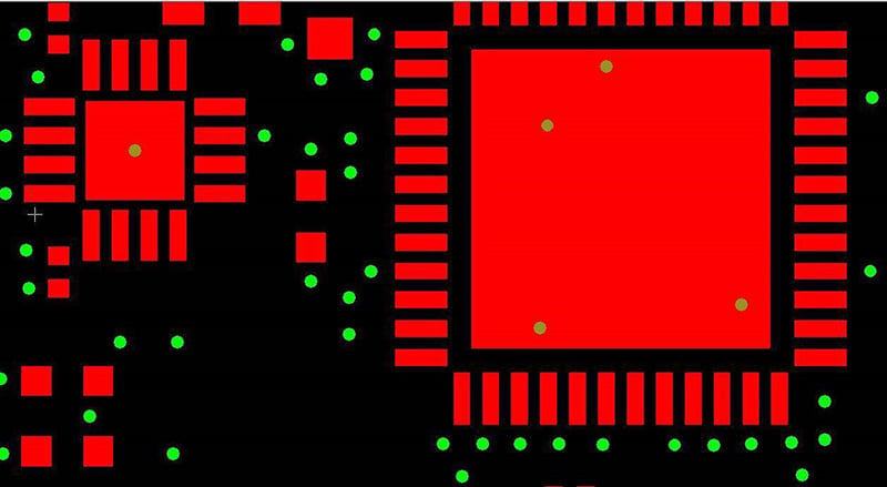
Read MoreAs printed circuit board (PCB) technology has been on a steady incline for many years, the main focus has been on what else can we make this part do. Add more layers, decrease circuit widths, add more components, buried vias, blind vias, control the impedance – the list of changes in technology is lengthy. As a manufacturer of PCBs, we see the finished design ready to go to production, but is it? Often, we look at a received customer data production and think, “can this part be produced?”
Read MoreAt the conclusion of our webinar, Quick Turns PCBs – Why an Experienced Supply Chain Matters - we had several questions submitted to our presenter, Ed McMahon, CEO at Epec. We have compiled these questions into a readable format on our blog.
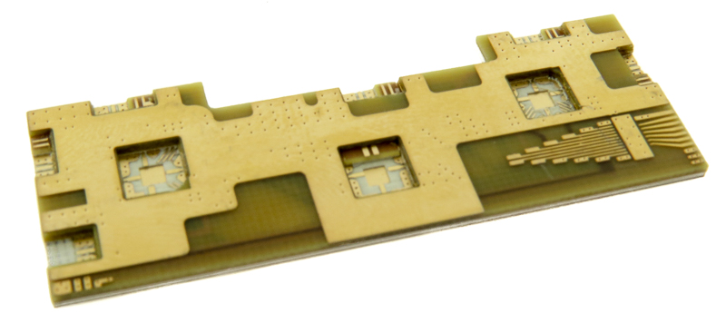
Read MoreThe talk about creating high-speed digital circuits is happening across the world due to the development of fifth-generation (5G) cellular communication systems. As technology becomes more advanced, engineers are looking for the right ways to convey signals and frequencies through standard materials that are available today for printed circuit boards (PCBs), as these PCBs need to handle the mechanical and electrical properties required without hindering operational capabilities.
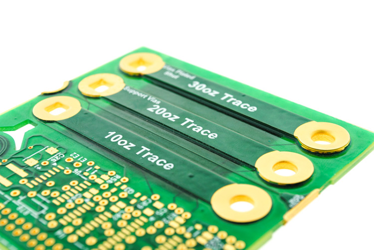
Read MoreDesigning a PCB with extreme copper plating requires planning and careful consideration of several factors that do not come up during the design of a standard, light copper board. Many fabricators avoid heavy and extreme copper circuit board orders entirely because of the unusual manufacturing challenges and non-standard processes associated with these product types.
Read MoreFront panels, bezels, and other types of human to machine interface equipment use several circuit technologies to operate. These circuit types usually involve some form of printed or etched traces using conductive materials like copper and conductive ink. These custom layouts are routed across insulating sheets and films, eventually becoming circuit boards and flex circuits. Dome switches, LEDs, and touchscreens can be added to these everyday circuit boards, bringing them to life as a high-technology HMI solution.
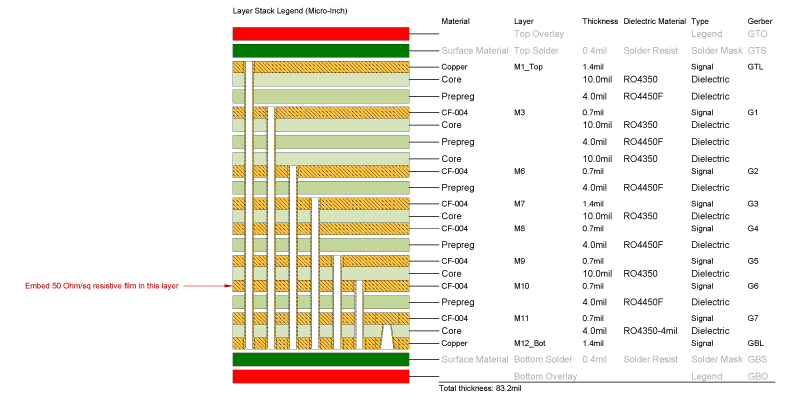
Read MoreWhen you are designing a printed circuit board (PCB), your customer or boss does not typically hand you a blank check. You may occasionally be fortunate enough to have a customer with deep pockets, but most products are very cost-sensitive, and your board design will need to come in at or below budget. This post will go over some of the things you can do to achieve a cost-effective design. Its focus will be limited to a handful of higher-end design options.
Read More


