After an engineer has finished their circuit design for a printed circuit board (PCB), the next step is to enter the schematic details into a computer-based schematic capture program such as Altium, Eagle, or OrCAD. The finished printed circuit board will provide the physical assembly and interconnection platform for the various electronic components required by the schematic.
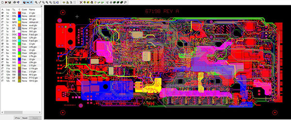
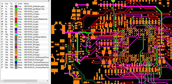
The schematic capture program provides detailed information about the completed board design in a series of data (Gerber) files for each conductive layer of the PCB.
The Gerber file is the most important item for fabricating a circuit board. These files were initially developed by a company called Gerber Scientific, founded by Joseph Gerber, and have become the traditional format for consistent production of circuit boards.
Gerber File Processes
The Gerber files are typically zipped into a single file and sent to the printed circuit board manufacturer. At times, the data package will consist of multiple layers, depending on the stack-up of the PCB, drill programs, assembly, pick and place, fabrication drawings, and array layout. Each artwork layer, copper circuitry, power, or ground must have a corresponding Gerber file to create the required pattern.
The outermost layers, referenced as “top” and “bottom,” component and solder or by layer count will also have a conforming layer for solder mask and silkscreen to be applied. A paste layer or layers are typically provided for assembly purposes and matching step and repeat of the array layout.
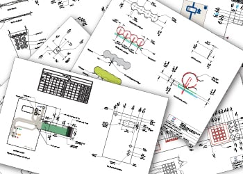
Files for programming drilling machinery are also provided; some of the time multiple sets of drill files are needed for the manufacturing of the part. The drill program provided for each hole is a X, Y coordinate that is related to 0,0 as shown within the data and on the fabrication drawing. Many times, non-plated holes, slots, blind and buried vias, and plated through-holes are indicated in different files. There should be a detailed board outline 1:1 describing the machining profile to be produced and any internal cutouts to be made. Often included is a README.txt file, which states the purpose of the above-mentioned files. It also is suggested that a fabrication drawing is exported as a Gerber file.
The file names for the Gerber files are often descriptive enough for the PCB manufacturer to understand which board and board layer each file applies to. Supplying a corresponding stack-up marked as the Gerber’s are labeled within the zip file is advantageous to engineering when laying out the part for production.

Gerber files have become the traditional format for consistent production of circuit boards.
Files are named with extensions such as .TOP and .BOT or .SMT and .SMB are often used instead of the .GB_ type extensions. The file extension for a type of file, top, bottom, silkscreen, paste, inner layer, is controlled by the PCB CAM software package or is selectable within the package.
The CAM engineering software used by the manufacturer to create the circuit boards utilizes manufacturing data to create two-dimensional or three-dimensional designs of the PCB. They receive all the information needed from the Gerber files in order to etch the copper layers, create the component pads and connection traces, drill all required holes, and profile the board to the required size.
The Gerber data is imported into these CAM systems to produce the designs for production. Upon import the files are labeled accordingly, set to 0,0 archived and saved in the original format. The engineer will manipulate the files for production ready layout, singles or within an array. Clean up is critical to processing files correctly in production. Design rule checks are set to parameters for the type of PCB being checked. Manual and automated cleanup are performed on each layer during the cleanup the engineer will compare to the archived original files to be sure no electrical changes have occurred.
Engineers must refer to guidelines and references mentioned in the Gerber file while entering manipulating the data. A Gerber file is developed such that it elaborates the requirements in each stage of the product development. These files are used for both processes: PCB fabrication and PCB assembly.
Gerber File Formats
RS274-D
The oldest format of Gerber file designed by Gerber Scientific. The file was represented in the numerical control (NC) format, and it was compatible with different photo plotters used in the 1970s. Due to several drawbacks of this format, manual input of d-codes, user interpretation, other types of Gerber files have been developed since. This format was known as the Standard Gerber.
RS274X
This Gerber file format has been used since 1998. This revised format of RS274-D utilizes an embedded format, unit and data information. The apertures defining the layers are embedded allowing for standard sizes and custom apertures. In addition, the RS274X format allows the designer to utilize film control, multiple layer structure for single layers, special polygon fill commands, polarity controls, and much more. The improved format eliminated the manual data entry and reduced the photo plotting errors to a rarity.

Gerber file format RS247X has been used since 1998.
ODB++
Developed by Valor to be an all-inclusive, self-extracting, and standardized input format, automating the process for stack-up, drill placement, and labeling. Initially not user friendly by other software programs, ODB++ can now be input by most CAD programs. ODB++ removed additional room for human error, manual naming conventions the zip contains all design and fab information as well as netlist data. A good format is not preferred by all, but useful in the industry.
Gerber X2
This is the newest Gerber format and is designed for most advanced CAM software applications. This allows for certain attributes to be assigned to features within the Gerber file that are interpreted and implemented by the CAM software, providing additional information for the fabricator and the CAM operator. Some example attributes that can be applied within the Gerber file are:
- Function of file (Top mask, top copper, etc.)
- Part represented by the file (single PCB, an array, coupon, etc.)
- Function of pad (SMD, Via pad, fiducial, etc.)
The X2 format is compatible with its original X1 format, allowing for the designer to transfer valuable design information to the Gerber.
Summary
As a design engineer at Epec who works with legacy user interface products, I often review PCB drawings that include the various Gerber file layers. The CAM engineers on our team are excellent at providing information on the files, as well as updating them when changes are needed. The Gerber files are an essential part of the printed circuit board manufacturing process. Understanding the manufacturing process, manipulation of the data, layout, and streamlining the process for continued excellence in manufacturing PCBs is what Epec does best.
Key Takeaways
- Gerber files are essential for PCB manufacturing: They contain detailed layer-by-layer information of a printed circuit board design, including copper layers, solder masks, silkscreens, and drill data used for both fabrication and assembly.
- Each PCB layer and function has a corresponding Gerber file: Files are organized and labeled to match specific board functions—like top copper, bottom solder mask, and drill programs—and are often zipped together for submission to manufacturers.
- There are multiple Gerber file formats, with RS274X being the most common: RS274X is widely used due to its embedded design data, reducing manual input errors. More advanced formats like Gerber X2 and ODB++ provide extended design metadata and automation benefits.
- CAM software translates Gerber data into manufacturable layouts: Engineers at the fabrication house import and clean up the files, run design rule checks, and prep the board for panelization and production, ensuring accuracy and performance.
- Accurate Gerber data streamlines production and minimizes errors: Whether you're building a single board or an array, well-organized Gerber files reduce production delays, prevent mistakes, and ensure the final PCB matches the design intent.


