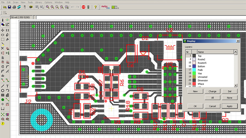
Ordinarily you may not want your PCB (printed circuit board) manufacturer to adjust your data files, but there are occasions when that may be the easiest way to achieve a particular result. For instance, you may need to have some, but not all, vias of a particular size plugged so that the assembly solder will not wick through to the other side of the board. Or perhaps a few trace pairs need to run at a specified impedance, while the impedance for all the other traces of the same width is non-critical.
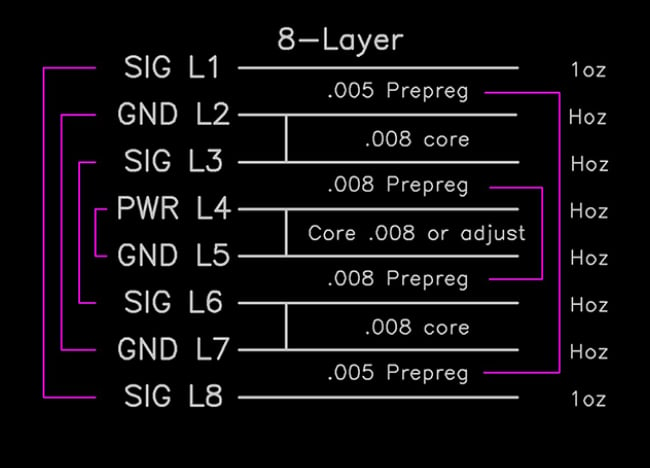
Read MoreThe design of a multi-layer PCB (printed circuit boards) can be very complicated. The fact that a design even needs to use more than two layers implies that the required number of circuits will not fit onto just a top and a bottom surface. Even in cases where the circuitry does fit onto two external layers with no problem, the PCB designer may decide to add power and ground planes internally in order to correct a performance shortcoming.
Read MoreOwing to the prevalence of complex processors, USB devices, and antennas printed directly onto the board surface, more and more PCB designs now require impedance control and testing than ever before. In response to the increased demand, circuit board manufacturers have invested in sophisticated modeling software and testing units, so they are equipped to meet the requirements.
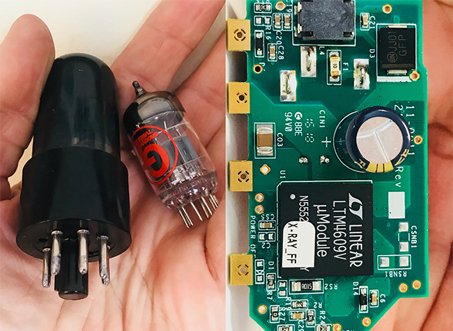
Read MorePrinted circuit boards (PCBs) have become an integral part of everyday modern life, both at work and at home. PCBs were at one time found primarily where you would have expected them to reside inside computers, calculators, televisions, and other such obviously electronic devices, but now they present nearly everywhere.
Read MoreIt is sometimes necessary to have some, or all, of your PCB layout projects done by an outside source. If you’ve never done a layout before, or if you don’t have the tools or experience to take on more complex projects, it is often better to have a professional complete the work.
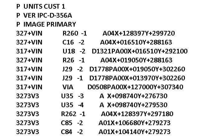
Read MoreNobody wants to experience the feeling of populating your new printed circuit board (PCB) design and finding out that it is not electrically functional. Most often, the lack of functionality is attributable to a specific production problem or a combination of several different problems. Sometimes, however, the problem is that the Gerber files exported from your PCB CAD program contained an error that went unnoticed because there was no way to verify that the files matched your design intent. You can avoid a good deal of trouble by supplying an IPC-356 format netlist file with your fabrication data package.
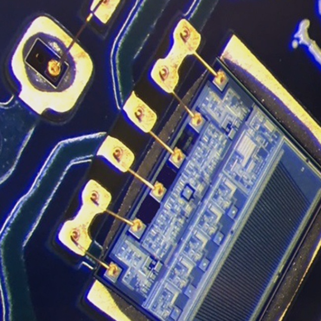
Read MoreENEPIG (Electroless Nickel, Immersion Palladium, Immersion Gold) was derived out of the need to combat the challenge with the immersion gold process and Black Pad Syndrome. Black Pad (the hyper corrosion of underlying nickel) was baffling both PCB assemblers and manufacturers. After much analysis, the root cause was determined to be the nickel deposit.
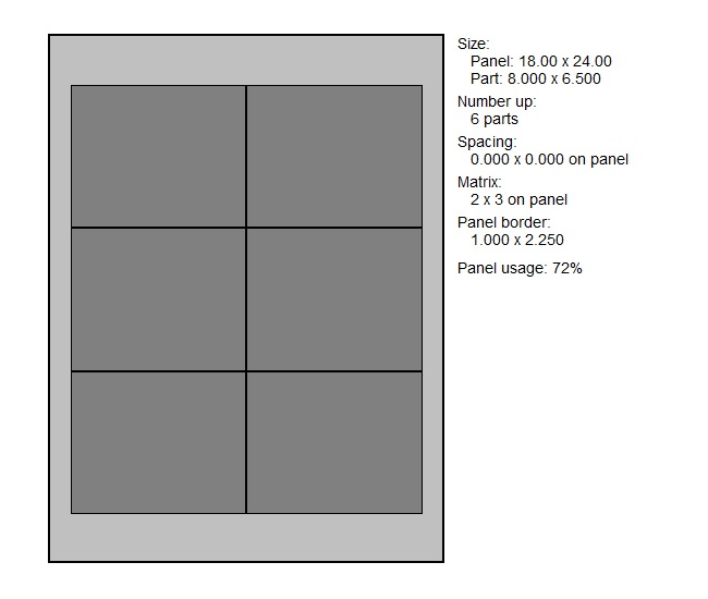
Read MoreAs costs of materials, freight, and labor rise it has become imperative to seek out alternative ways to save costs in the manufacturing process. With traditional means of saving no longer as viable, we now must be more creative and specific when we’re asked, “what can I do to lower the cost of my printed circuit board (PCB)?”
Read MorePrinted circuit board (PCB) designers often find themselves at odds with their purchasing and marketing departments after a design goes out for bids and comes back with a larger than expected price tag. Once the source of the high cost is identified, the questions fly, the fingers point, and the nerves fray.
Read MoreWhile gold plating is frequently used for printed circuits boards (PCBs), selecting the most useful gold PCB surface finish can be somewhat more of a mystery. Understanding the different compositions and practical uses of gold finishes such as ENIG, ENEPIG, and gold fingers can help you find the right finish to match your circuit board needs.
Read More


