



V-scoring remains one of the most widely used methods for panelizing printed circuit boards (PCB) and preparing them for depanelization after assembly. As PCB manufacturing technologies continue to evolve, designers should understand the design constraints that affect whether a circuit board is a good candidate for scoring and when alternative approaches such as routing may be more appropriate.
The scoring process uses two opposing blades that rotate point-to-point while the PCB passes between them. The blades create matching grooves from the top and bottom surfaces of the circuit board, leaving a thin web of material that allows individual boards to remain connected during fabrication and assembly while still being separable later. A 30° blade angle is commonly used for PCB V-scoring, although other blade angles may be selected depending on the board construction and scoring requirements.
Although scoring is an efficient and commonly used process, board thickness, panel design, board geometry, material selection, and depanelization requirements can affect its success.

When Is a PCB a Good Candidate for V-Scoring?
Printed circuit boards with straight edges and rectangular or square outlines are generally the easiest to process using V-scoring. Straight circuit board edges allow the scoring blades to pass continuously across the panel without interruption.
However, a circuit board having straight edges alone does not automatically make it an ideal scoring candidate. Additional factors such as thickness, size, array strength, and edge clearances should also be evaluated.
Why Thin PCBs Can Be Difficult to Score
Printed circuit boards thinner than 0.040" can present challenges during both scoring and depanelization. Although V-scoring may be possible on boards as thin as approximately 0.031", depending on the material, construction, and manufacturing capabilities, 0.040" is a practical minimum guideline for standard scoring applications.
A standard scoring process requires a minimum web thickness to remain after scoring. To maintain a V-score web, approximately 0.012" of remaining material is required. When score blades are set to cut 0.010" to 0.012" deep from both sides of the board, the resulting web is approximately 0.020" ± 0.004".
As board thickness decreases, controlling this remaining web becomes more difficult. Thin PCBs also exhibit greater material flexibility.
During separation, this can result in:
- Rough board edges
- Hanging fibers
- Uneven breaks
- Edge fracturing
Score depth accuracy becomes increasingly important because any imbalance between the top and bottom scores can make separation more difficult and increase the likelihood of cosmetic or structural edge damage.
For printed circuit boards less than 0.040" thick, routing with tabs is recommended instead of scoring.
How Array Design Affects Scoring Success
Panel strength decreases as additional score lines are added. Each score line removes material from the panel and can weaken the overall array structure.
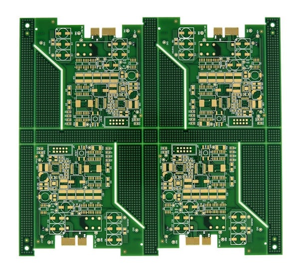 Odd Shaped Circuit Board Scored in Array
Excessive scoring may lead to:
- Fragile panel handling
- Premature panel breakage
- Assembly-related issues
- Transportation damage
When developing panel layouts, the number and placement of score lines should be evaluated along with the mechanical strength required throughout fabrication and assembly.
Challenges With Small PCB Designs
Board size can significantly affect depanelization performance. As the overall square-inch area of a PCB decreases, separating scored parts becomes more difficult. This issue becomes more pronounced when board thickness increases.
For example, circuit boards approximately 0.062" thick or greater can be difficult to separate when the board is very small. Designs measuring less than 1 inch in any direction may require specialized separation tools to achieve clean depanelization.
Long Circuit Boards Can Become Structurally Weak
Circuit boards with a long X or Y dimension require additional consideration when using scoring.
Printed circuit boards measuring 12 inches or longer in either direction can become more susceptible to breakage when score depth is excessive. The risk increases further when heavy components are installed on an already weakened panel.
In these situations, panels may crack or separate during:
- Handling
- Assembly operations
- Shipping and transportation
For longer circuit boards, jump scores or tab routing may provide better panel integrity.
Considerations for Thick PCBs
Scoring also becomes more challenging as board thickness increases.
With circuit boards thicker than 0.096", the scoring blades must penetrate deeper into the laminate while still maintaining the target web thickness of approximately 0.020" ± 0.004". As material thickness increases, separating the remaining web becomes more difficult because the laminate provides less flexibility.
The result can be:
- Difficult depanelization
- Hanging fibers
- Uneven edge appearance
- Torn-looking edge surfaces
Although thicker scoring blades can be used to process thicker boards, doing so may introduce constraints related to copper-to-edge spacing requirements.
Depanelization Tools Require Careful Use
Various depanelization tools are available to assist with separating scored boards. However, tool selection alone does not eliminate risk. Improper use or insufficient process control can damage assembled boards through:
- Edge damage
- Surface scratching
- Fracturing
Because depanelization occurs after assembly, every additional handling operation introduces some level of risk to the finished product.
Can Angles and Radii Be Used with Scored PCBs?
Angles and radii do not automatically prevent the use of scoring, but straight edges are still required where score lines are applied.
In a typical scored panel, circuit boards are placed directly adjacent to one another and are separated using the scoring blades. When angled edges or radiused features are introduced, routing becomes necessary to create the desired geometry.
A typical router uses a 0.096" cutting tool, requiring at least 0.100" spacing to route cleanly between adjacent circuit boards.
While 0.100" spacing may be sufficient for routing, it is generally not recommended when boards must also be separated using scoring because depanelization becomes extremely difficult. When spacing between boards is required, 0.200" or greater is recommended when scoring is part of the panelization strategy.
Design Guidelines for PCB Scoring
Most printed circuit boards with straight edges can be scored successfully, although some designs benefit from a combination of scoring and routing.
Adjust Scoring for High-Tg Materials
Higher-temperature laminate materials above 150 Tg have a denser structure and weave than standard 130 Tg materials.
Standard scoring parameters used for 130 Tg laminates should not automatically be applied to these materials. A deeper score is generally required to allow cleaner separation.
For higher-temperature materials, use a web thickness of 0.015" ± 0.004".
Maintain Adequate Metal-to-Edge Clearance
Copper and other conductive features should be kept an appropriate distance from the finished board edge.
For printed circuit boards 0.062" thick or less, maintain a minimum clearance of 0.015" from the finished edge.
For thicker boards in the 0.096" to 0.125" range, 0.020" or greater clearance is recommended whenever design constraints allow.
Proper clearance helps reduce the risk of damage to conductive features during scoring and depanelization.
Consider Routing for Very Thin Designs
For printed circuit boards thinner than 0.040", routing with tabs should be planned from the start of the design process to avoid the manufacturing and depanelization challenges associated with scoring thin materials.
Selecting the Appropriate Depanelization Strategy
V-scoring can be an effective and economical panelization method when the board geometry, thickness, material selection, and assembly requirements support its use. However, scoring is not the best solution for every design.
Thin boards, thick boards, small PCB formats, long panels, high-Tg materials, and designs containing radii or irregular outlines may require modifications to the panel strategy or a combination of scoring and routing. Evaluating these constraints early in the design process can help prevent depanelization problems and improve manufacturing efficiency.

Summary
If you still have doubts about how to best score your printed circuit board, don’t hesitate to consult your PCB layout engineer. If you don’t have this resource available at your company, we would be glad to have our engineering team help you determine the best solution for your needs. Our free DFM service is always available and we will be happy to make suggestions for panel layout and what you should do next.
PCB Manufacturing Explained: The V-Score & Jump Scoring Process
Key Takeaways
- V-scoring works best for boards with straight edges and adequate thickness: A board thickness of 0.040" or greater is a practical guideline for standard V-scoring, although thinner boards may be possible depending on manufacturing capabilities. Thin boards are more susceptible to rough edges, difficult separation, and breakage.
- PCB size, shape, and array design influence score effectiveness: Small boards (under 1 inch), long boards (12 inches or more), and odd-shaped PCBs may require a combination of scoring and routing for clean separation.
- Material type affects scoring depth: High-Tg laminates above 150°C require deeper scoring than standard 130°C materials to ensure a clean break due to their denser weave.
- Metal-to-edge clearance is critical: Maintain at least 0.015" clearance for boards 0.062" thick or less, and 0.020" or more for thicker PCBs to prevent damage during scoring and depanelization.
- Consider routing for very thin boards and complex designs: Circuit boards under 0.040" or with radii and angles often need routing with adequate spacing (0.200" recommended between parts) instead of or in combination with scoring.