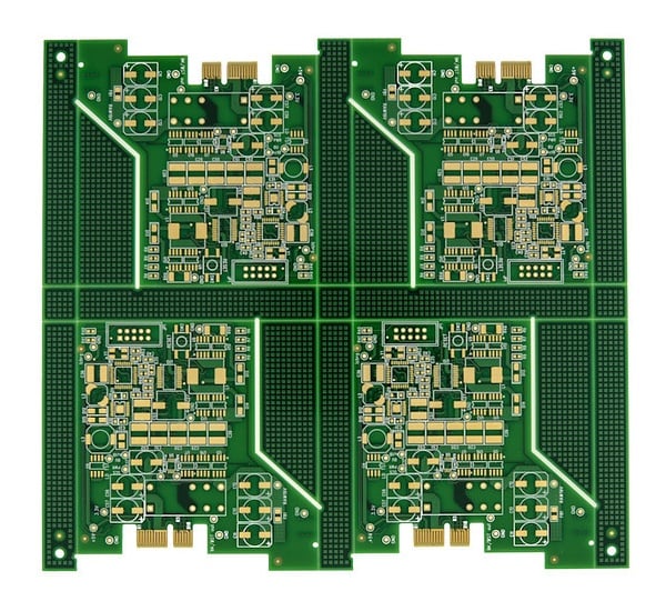
The process of v-scoring has been used for many years in the production of printed circuit boards (PCBs). As PCB production technology rapidly advances, it is important to understand the most current PCB scoring guidelines to follow and how they may have changed from what you previously used.
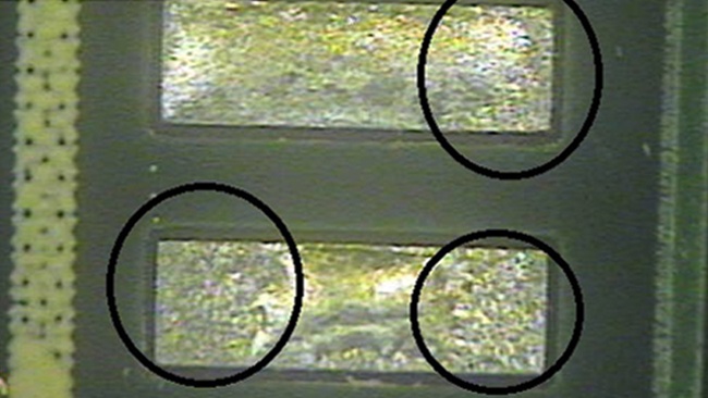
Read MoreSolving solderability issues for printed circuit boards (PCBs) can be a real hassle. Nothing is more frustrating than having lined up all your materials for an assembly, only to start running the package through reflow and discover that the solder paste is wetting poorly to the pads. Immediately, the profile is checked to confirm proper parameters.
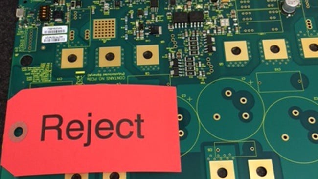
Read MoreFor customers and suppliers along the PCB manufacturing process, non-conformances will, unfortunately, happen from time to time. A non-conformance consists of receiving an order for printed circuit boards that do not meet your specifications or industry (IPC) standards. While dealing with these issues is obviously essential, the solution is sometimes not obvious and can put on-time delivery to your customer at risk. It is imperative that your circuit board supplier can deliver conforming product as soon as possible, which means having the procedures to get there.
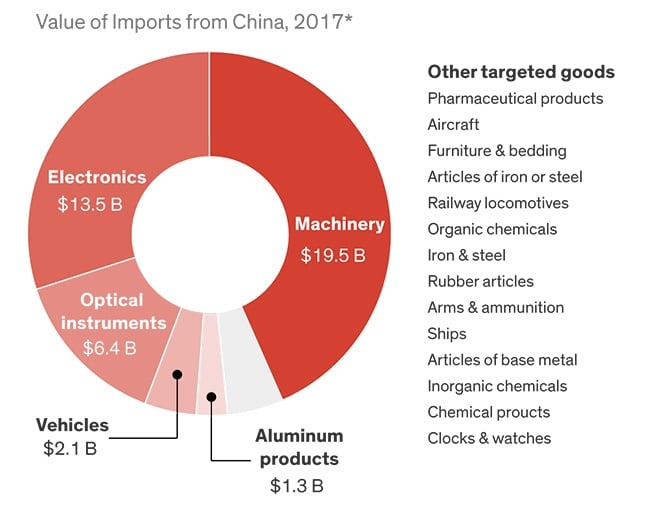
Read MoreTariffs and trade with China has been a hot topic in the news recently. The tariffs impacting the steel and automobile industries have been widely covered but there are many additional industries that could potentially feel the effects of these tariffs, including our own.
Read MoreIn front-end engineering, we must gather as much manufacturing information as possible from the printed circuit board data we receive. This includes customer service notes, customer emails, and the general spec, if available. Usually there is enough information to release a printed circuit board (PCB) package to manufacturing. However, I have found many gray areas that haunt our engineering department.
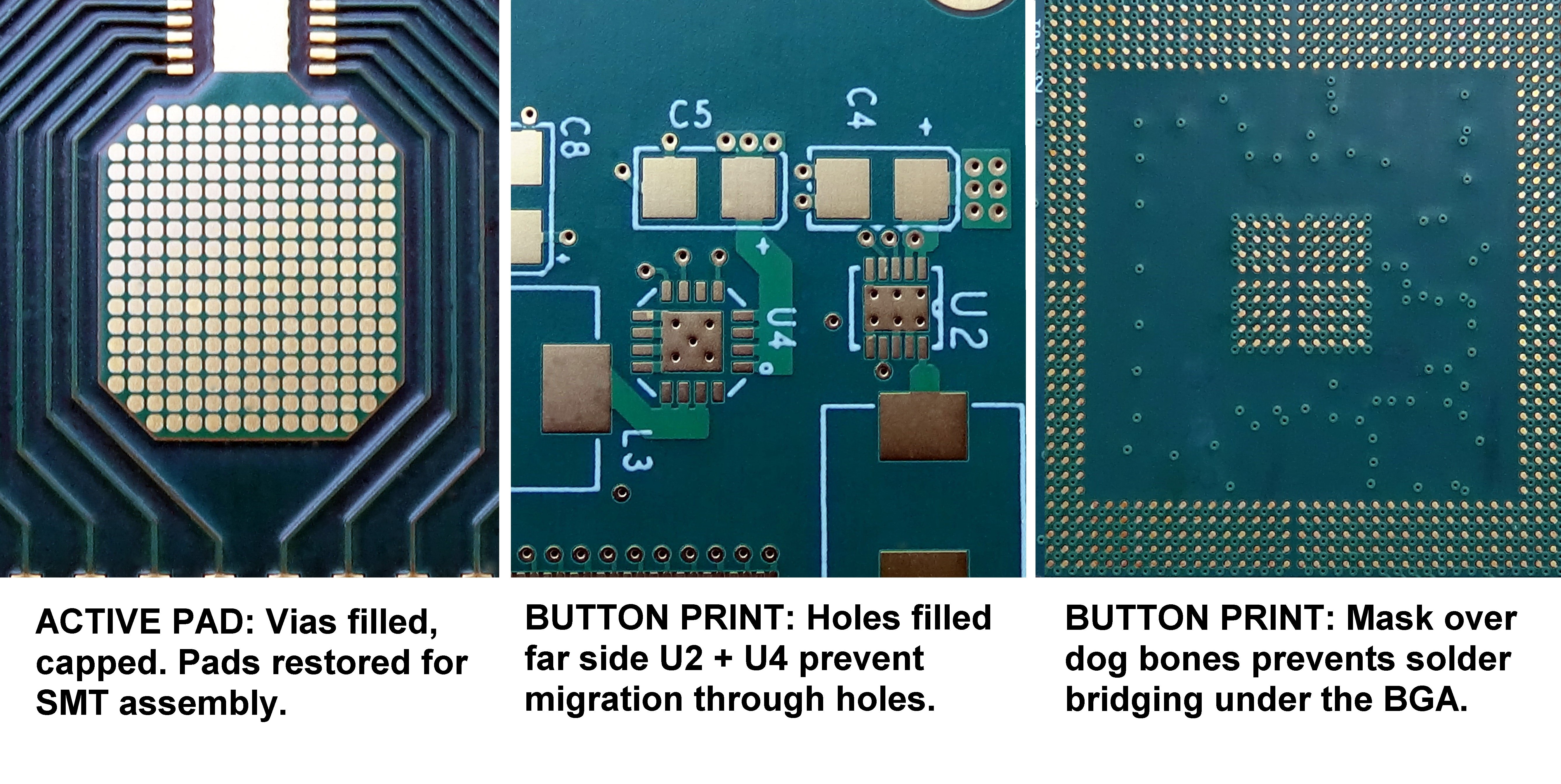
Read MoreAs today’s printed circuit boards (PCBs) become smaller, they use fewer and fewer through hole components. It is increasingly difficult to justify allocating precious space for relatively large plated through component holes and their accompanying lands. Instead, it is necessary to use surface mounted components wherever possible. As surface mount technology becomes increasingly prevalent, the majority of the plated through holes on most modern PCB designs end up being vias.
Read MoreAmong the most common questions printed circuit board suppliers receive are those dealing with production capabilities. Customers often suspect that they are about to design-in a feature which may be either at or outside their fabricator’s limits. Fearing that their non-standard feature may add cost to their product, they inquire to find out just how much pain they are about to cause.
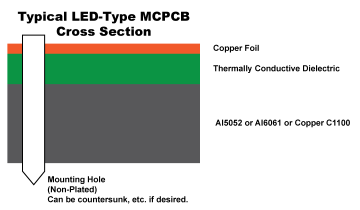
Read MoreOver the past several years LED based products have become increasingly popular, and as a result, so too have metal core printed circuit boards. The automobile and lighting sectors have both embraced the technology, as have consumers, given an LED based light can be about 5x cheaper to run than a comparable incandescent unit. Even compact fluorescents have slightly higher operating costs, and they cannot compete with the smallest LEDs when it comes to efficient use of space.
Read MorePrinted circuit board (PCB) fabricators receive dozens of requests for quotations (RFQs) every day. While many requests have moved to more convenient online quoting formats such as our in-house application InstantPCBQuote, many customers still send requests the old way via either files or alternate forms of describing their manufacturing requirements.
Read MoreSelecting PCB core thickness becomes a problem when a printed circuit board (PCB) fabricator receives a request for quotation of a multilayer design and the material requirements are stated either incompletely or not at all. This sometimes occurs because the combination of PCB core materials used is not critical to performance; if the overall thickness requirement is met, the end user may not care about the thickness or type of each layer.
Read More


