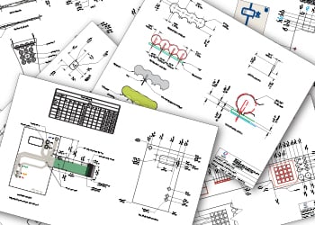




Many OEM engineering teams continue to face the same challenge: aggressive development schedules combined with limited engineering resources. As organizations ask engineers to handle a wider range of responsibilities, printed circuit board (PCB) layout projects can become a bottleneck that delays product development and product launch schedules.
Outsourcing PCB layout and design can help organizations expand design capacity, accelerate development, and improve manufacturability without increasing internal headcount. When selecting a PCB layout partner, several factors can have a significant impact on project success.

Circuit Board Layout Designed With Tight Spacing
How Extended Engineering Coverage Can Reduce Development Delays
A large portion of PCB layout work occurs between customer reviews, design updates, and technical discussions. While communication often takes place during normal business hours, layout activities can continue outside those hours when engineering resources are available.
This extended engineering coverage helps reduce idle time that can occur when a design is waiting for the next revision cycle or customer response. Even short delays can accumulate over the course of a project, affecting development schedules and time-to-market objectives.
For organizations working against aggressive deadlines, maintaining progress on PCB layout activities whenever possible can provide a measurable scheduling advantage.
Why Experience Across Multiple PCB Projects Matters
No two PCB layout projects are identical. Component selection, board architecture, performance requirements, mechanical constraints, and manufacturing considerations can vary significantly from one design to another.
Engineering teams that work across a broad customer base gain experience with a wide range of PCB layout challenges, design tools, and component technologies. That experience can help teams respond more efficiently to customer requests and design requirements.
Relationships with component manufacturers can also be valuable. Familiarity with components from suppliers such as TI, Microchip, Atmel, NXP, and others can help engineers better understand device-specific considerations that may influence layout decisions. Small choices involving component placement and implementation can affect overall circuit performance, making component knowledge an important part of the design process.

Organizations that support multiple PCB programs also benefit from the internal sharing of design knowledge and PCB layout best practices. Lessons learned from one project can often improve execution on future projects.
Define Project Goals Before Layout Begins
Successful PCB layout starts with a clear understanding of project objectives. Different priorities lead to different engineering decisions, and identifying those priorities early helps ensure the layout process aligns with business goals.
When Time-to-Market Is the Priority
Some products must move quickly through development, regulatory approval processes, and production schedules. In these situations, engineering teams may favor proven components over newly released alternatives to reduce development risk and avoid unnecessary delays.
When Cost Is the Primary Driver
Projects focused on cost control require ongoing evaluation of how design decisions affect the final product cost. Even seemingly minor engineering changes can influence overall manufacturing expenses. Design teams should communicate those impacts early so that technical decisions remain aligned with cost objectives.
When EMI or RF Performance Is Critical
Applications operating in environments such as emergency rooms, data centers, or aircraft may face significant EMI or RF performance requirements. Certain applications may require compliance with specific testing requirements before they can be considered acceptable for deployment.
PCB layout is an important stage for addressing these challenges because it is where engineers can evaluate and implement strategies intended to support the project's performance objectives. Discussing EMI and RF requirements early in the layout process helps establish an appropriate design approach before manufacturing begins.
Designing for Manufacturability from the Start
PCB layouts must be more than electrically functional. They must also be practical to manufacture.
Working with organizations that have both PCB layout and PCB manufacturing experience can help improve manufacturability by incorporating production considerations earlier in the design process. This approach may reduce the likelihood of preventable manufacturing issues, redesigns, or production-related revisions.
When manufacturing requirements are considered during layout, the transition from design to production can be more efficient and predictable.
Potential Cost Advantages Beyond PCB Design
Some PCB layout and design providers also offer PCB manufacturing services. In these cases, customers may receive pricing advantages when the same supplier performs both the layout work and the PCB fabrication effort.
Beyond potential cost savings, consolidating design and manufacturing activities with a single provider can simplify project coordination and communication throughout the product development cycle.
Summary
Outsourcing PCB layout and design can be an effective way to expand engineering capacity, maintain project momentum, and support aggressive development schedules. Organizations that partner with experienced PCB layout providers may benefit from broader design experience, earlier consideration of manufacturability requirements, and engineering decisions that align with specific project goals.
When resources are limited and time-to-market is critical, selecting the right PCB layout partner can help reduce development challenges while supporting overall project objectives.
Key Takeaways
- 24/7 engineering support maximizes efficiency: Outsourced teams can continue PCB layout work after business hours, preventing costly delays in tight development schedules.
- Broad customer and component experience adds value: Working with multiple OEMs and component suppliers equips design firms with best practices and insights that can improve every project.
- End goals drive design decisions: Whether the priority is speed to market, cost control, or EMI/RF compliance, experienced engineers tailor layout strategies to meet specific objectives.
- Manufacturability is built into the design: Partnering with firms that also manufacture PCBs ensures layouts are optimized for production, reducing risk and revisions.
- Potential cost savings extend beyond design: Many design houses offer manufacturing discounts when they also build the PCB, further reducing overall project expenses.