As printed circuit board (PCB) designs have increased in complexity, they have both decreased in size and increased in density. Physical changed to circuit boards have forced PCB designers and manufacturers to develop new PCB layout strategies aimed at making full use of all available surface area.
With greater density boards, there becomes a greater difficulty in fabricating the raw PCB, as well as assembling the board once it gets built. It is important to understand how decisions at the design level will affect the later manufacturing stages, and to then determine the best design practices which will result in a successful manufacturing experience.
Below is a brief examination of how two important factors, via treatment and circuit spacing, can have a large impact on the success of a project.
Printed Circuit Board Vias
Printed circuit board vias are generally covered by solder mask or filled with epoxy and sometimes (as with dense BGAs) capped to recover the surface for soldering.
Different PCB designs may require different treatment options. To understand how to identify the best via treatment for each situation, familiarize yourself with the various options described in IPC-4761. Talk to your contract manufacturer (CM) and your fabricator during the design stage because not every CM has the same preferences.
It is not unheard of for two different CMs to source the same original equipment manufacturer (OEM) board from the same bare board fabricator with each CM specifying a different method for treating the vias based on their own preferences and process controls.
For example, leaving the vias at the ends of “dog bone” escape routing traces under a BGA will increase the likelihood of solder shorting under the BGA during assembly. This in turn increases rework and disrupts throughput. Most assemblers will want at least the pads for these vias covered by solder mask, while others may prefer that they be fully plugged.
Once you have established the best method for dealing with the vias, set up your solder mask layers to accurately reflect the desired finished product.
If your vias must be covered by solder mask, then remove the clearances from the top and bottom mask layers. If the vias will be plugged, it is best to supply one or two dot pattern Gerber files on unused mechanical layers to indicate which holes should be plugged and from which side.
This is less important if ALL the vias of a certain diameter are to be plugged because CAM engineers can create a plug layer without difficulty by filtering for that drill size. If the plugging is to be applied to a subset of the vias, supplying layers to your fabricator will save editing, eliminate errors, hold notices, and misinterpretations.
Printed Circuit Board Trace Widths and Spacing
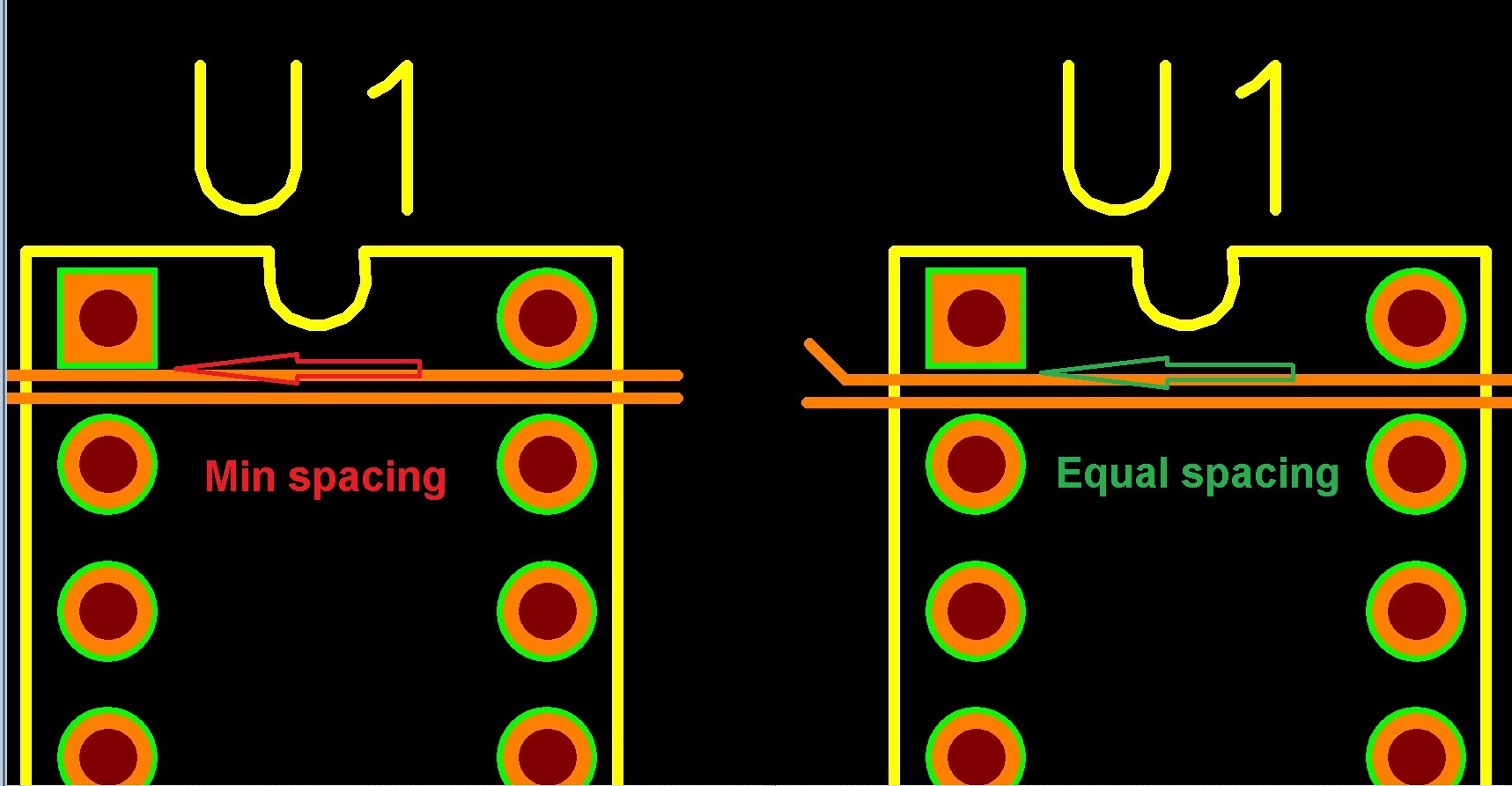
If you can design your PCB with more than the minimum spacing allowed by the fabricator, you will increase the processing window and reduce scrap. All fabricators have published limits for PCB trace width and spacing that they can produce consistently at acceptable scrap percentages, but it never hurts to provide more than the absolute minimum whenever possible.
For example, if a printed circuit board uses one small, tight component that requires 0.004” copper-to-copper spacing, but the rest of the design is less dense, the engineer will sometimes set the CAD design rule for routing all of the circuitry at 0.004”.
While this simplifies circuit routing and is not technically wrong, it can make the board more difficult to produce, because instead of a small number of tightly-spaced features, there are now many areas where the fabricator has less wiggle room than would be ideal.
Tighter spacing at areas where it is not needed may increase the frequency of shorts caused by incomplete etching. More commonly, it complicates solder mask application.
As real-world production tolerances come into play, small positioning variations between the drill pattern, the circuit image, and the soldermask pattern will result in enough shift(s) to cause exposure of nearby circuit traces. These exposed areas can short after assembly as solder forms bridges between the pad and the unintentionally exposed circuit trace. This is why it is advisable to use wider design rules in areas where it’s not absolutely necessary to go to the minimum value.

PCB Minimum Spacing Copper to Copper
Summary
Keep in mind that the choices you make at the design stage will affect production of the printed circuit board, the PCBA, and even the finished product into which the PCBA is installed.
While it is worthwhile to familiarize yourself with industry specifications such as IPC-2221 and IPC-4761, your best resources are your board fabricator and your contract manufacturer.
We recommend that you discuss non-standard features with them; they will welcome the opportunity to provide input. The result will be a wider process window and a smoother manufacturing experience.
Key Takeaways
- PCB complexity drives new layout strategies: As boards become smaller and denser, design choices directly affect manufacturability and long-term reliability.
- Via treatment must be planned early: Options like covering with solder mask, epoxy filling, or capping need to align with IPC-4761 standards and the fabricators and assembler’s preferences to prevent issues like solder shorts under BGAs.
- Clear solder mask layer definition is essential: Designers should provide accurate mask layers or plug files to avoid misinterpretations, delays, or fabrication errors during CAM processing.
- Avoid minimum spacing where not required: While fabricators can produce fine traces, applying tight spacing across the entire design unnecessarily increases difficulty, scrap rates, and risks of solder mask misalignment or shorts.
- Collaborate with your fabricator and CM: Engaging them early ensures alignment of non-standard features, maximizes the process window, and minimizes downstream manufacturing risks.


