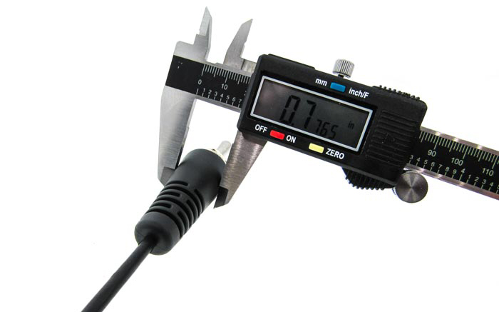
Scientists and engineers are sticklers about the units for any measurement, and rightfully so. The technique of using units' cancellation remains one of the fundamental concepts taught in all higher education STEM courses. Whether the course is chemistry, physics, thermodynamics, or even aerodynamics, the criticality of units is ever-present throughout lecture, calculations, and lab studies.
Read MoreAt the conclusion of our webinar – Design Considerations for Lithium Batteries Used in Portable Devices – we had several questions submitted to our presenter, Battery Development Consultant Randy Ibrahim. We compiled these into a readable format on our blog.
Read MoreEvery year, post Labor Day, most of us are focusing on getting “back to work” and recovering from whatever the summer holidays brought our way. As the weather starts to cool, and the sports start to change, those of us who work in supply chain management, procurement, and shipping immediately turn our eyes to what has become the constant fourth quarter challenge: getting our companies through peak season with no delays or surcharges.
Read MoreOvermolded cables are used in countless applications across almost every industry. The reasons to use an overmolded cable design are numerous, but the primary reason is to protect the electrical contacts while offering strain relief.
Read MoreAlthough they may not seem like much of a danger on a day-to-day basis, a lot of people don't realize that all batteries are technically considered to be hazardous by their nature when it comes to the topic of shipping them. This is why, if a consumer goes to the United States Post Office to ship a package, one of the first questions they're asked by a representative has to do with whether or not their parcel contains any items like batteries that could pose a problem during transportation.
Read MoreWhen using power sources to run embedded components, it's not always simple to pop in a fresh set of batteries. Newer technologies, from smartphones to electric vehicles to portable power tools, require batteries that can hold a significant amount of energy, be lightweight enough to carry or move, and be safe for the user. Lithium batteries offer all these benefits for portable electronics, vehicles, medical equipment, and even grid energy storage.
Read MoreBattery packs - especially rechargeable ones - are assets that we tend to take for granted until it's far too late. One minute your battery pack is operating at peak efficiency, the same as it always has. The next minute, it only lasts a fraction of the time it once did between charges and you just can't figure out why.
Read MoreWhen we talk about battery backup power systems for commercial settings, most people think about companies in the telecommunications, utilities, and healthcare industries in need of emergency sources of power when the electricity goes out. Yet, small and large companies require backup batteries for a range of operations.
Read MoreWhen you are designing a custom battery pack, it is always beneficial to understand the markets intended at the onset of the project. And as you would expect, a battery pack can be designed with several optional features that will ultimately add costs in the end. This blog post provides information on design while helping to keep costs aligned with your needs.
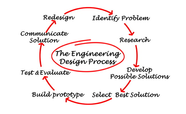
Read MoreAt Epec, engineers are expected to find innovative solutions to problems and develop them quickly and accurately so that customers can get quality products delivered on time. In this blog post, I will discuss how the 80-20 rule can be used in conjunction with our classic engineering design process to reach solutions faster.
Read More


