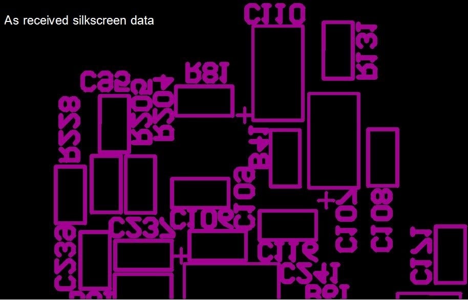
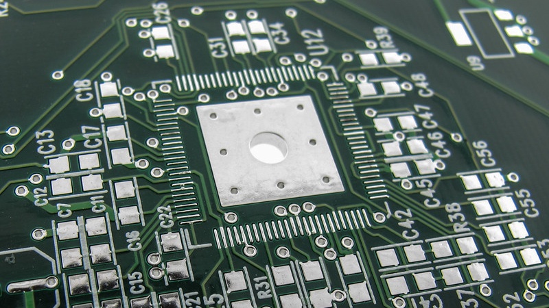
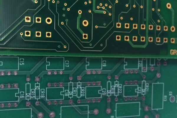
Among the multiple layers of a printed circuit board (PCB) lies the PCB silkscreen layer. The placement of the silkscreen markings, whether on the top or bottom layer, in conjunction with the features of the other layers, could affect the final legibility of the printed circuit board markings.
Read MoreEarly on in the printed circuit board (PCB) industry, "quick turn PCB" was a very relative term. Purchase orders were faxed, confirmed with a phone call, and lead time was open for discussion. Quick turn PCBswere 7-10 days, maybe as low as 5-days for a fast PCB manufacturer. A 2-day PCB quick turn was a very rare order which designated a person to move through production from process to process, bumping every other board from the line.
Read MoreHot Air Solder Leveling (HASL) has always been the main staple of PCB surface finishes. In the late 1980s, 60/40 tin-lead reflow started to phase out of processes and was replaced with Hot Air Solder Leveling. HASL finish, the long running reliable surface finish, is still used today in military, aerospace, medical, and other applications.
Read MoreWhen placing an order or requesting a quotation for printed circuit boards (PCB), it is extremely important to clearly state all of your requirements as completely as possible.
While this may seem obvious, it is surprisingly common for PCB fabricators to submit a pricing estimate to the customer based on information supplied within the request for quotation, only to receive additional information after pricing and delivery have already been agreed upon and a purchase order issued. If the new information affects the price and/or lead time, the fabricator must notify the customer of the changes in terms.
Read MoreTwo years ago I wrote about why printed circuit board (PCB) shops in North America were continuing to close. Now, in the last two weeks, we have seen two more shops (Dynamic & Proto and ITO Industries) cease their manufacturing operations.
As the former owner and operator of three domestic PCB facilities, I can sympathize with the management and the loyal employees that tried to make the company successful. However, much of the damage is self-inflicted as I previously discussed so rather than rehash past information I wanted to discuss some of the attributes that every customer should look for in their US PCB manufacturer.
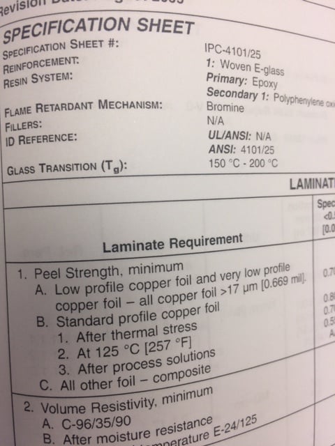
Read MoreIPC 4101 (Specification for Base Materials for Rigid and Multi-Layer Printed Circuit Boards) was released for publication in December, 1997. It was released as the replacement standard for MIL-S-13949. However, it contained a majority of the exact wording from the military standard. It maintained the “slash sheet” format appendix to the standard that specifies the resin and fiber system of different PCB laminates, along with testing parameters and properties. Initially there were 41 slash sheets, but as the industry opens up to “Lead Free” and “Green” processes, the slash sheets have increased to 66, the current revision.
Read MoreWhen it comes to manufacturing, time is of the essence. Worries about how fast your printed circuit board (PCB) order will arrive and whether it's on time is largely in the hands of the PCB manufacturer, but what can you do to to ensure the process moves as quickly as possible?
Choosing to work with a high quality quick turn PCB services supplier is obviously the first step. As the oldest existing printed circuit board supplier in the United States, not only can we help you construct highly reliable custom products, but we can give you the tips you need to ensure your PCB orders won’t get delayed.
Read MoreIn 2016 there were ten printed circuit board (PCB) factories that closed in the United States, including some highly sophisticated shops that were part of the TTM/Viasystems merger. Having been involved in the closing and transfer of part numbers for fifteen PCB facilities in the past twelve years, we have some first-hand advice as to how you can best minimize the risk as you change suppliers.
Read MoreAs a contract manufacturer, say you receive a new circuit board part to assemble that is 6-layers with a high micro-via count, has blind and buried vias, and a lead free HASL finish. The circuit board laminate requirement for meeting the Restriction of Hazardous Substances, or RoHS compliance, is strictly Glass Transition Temperature(Tg) 170.
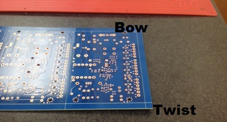
Read MoreBow and twist of printed circuit boards (PCB) routinely rank among the highest levels of falsely identified non-conformance because it is perhaps the least understood. Envisioning a perfectly flat rigid circuit board as the standard is a fallacy believed by many incoming inspectors. Understanding the reasons and causes for PCB bow and twist can help resolve the issue at the board design stage.
Read More


