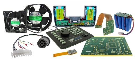
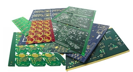
Epec Engineered Technologies is one of the oldest printed circuit board companies in the U.S., building PCBs since 1952. Epec is one of the founding members of the Institute of Printed Circuits (IPC), created in 1957 to help advance the PCB industry. While visiting a customer I was asked, “Has the introduction of your new products like custom battery packs and energy efficient EC fans taken your focus and attention off of PCBs?” While I assured the customer that we are fully dedicated to PCB manufacturing, it occurred to me that as a company, we need to better demonstrate that dedication consistently to our customers.
Read MoreHistory of PCB Manufacturing
When I started working in the printed circuit board manufacturing business 34 years ago, I believed it was a temporary job to pay the bills. Just until I was able to figure out what I really wanted to do. That was in 1982, working at a small PCB shop.
Read MoreAs printed circuit board (PCB) designs get more demanding with advances in technology involving complex footprints and added costs to components, incoming inspection of printed circuit boards must take higher priority.
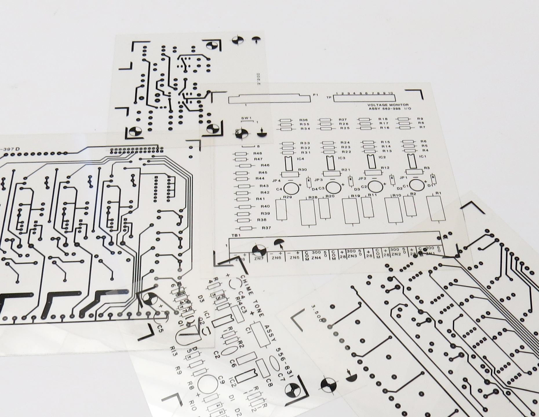
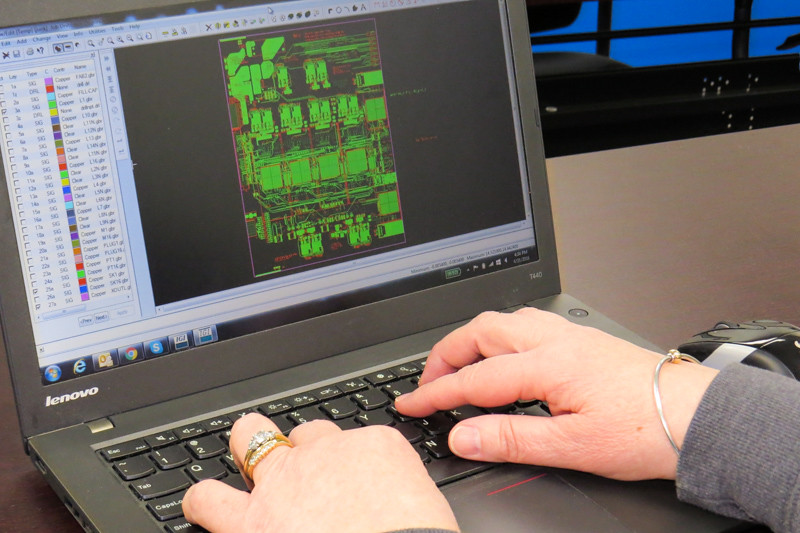
Read MoreEpec’s printed circuit board (PCB) engineering team is here for you 24 hours a day, 7 days a week. We have 6 full-time PCB CAM Engineers in the United States, along with 2 more full-time at our Shenzhen, China office. Our U.S. CAM Engineers work on 2 separate shifts, so we really do have assistance available 24/7 for all your PCB design and manufacturing needs.
Read MoreBack when laser drilling equipment was north of $1M, or when plasma etch equipment was so dangerous that it needed to be housed in a special room, only the largest companies could afford to purchase the equipment required to manufacture the highest technology printed circuit boards (PCBs). The only way to maintain good yields was to staff a squad of highly experienced engineers who understood the nuances of that specific facility equipment. Today, times and technology have changed dramatically to the point where this is no longer the case, allowing for more efficient mid-sized high tech PCB manufacturers to exist.
Read MoreYour PCB design for manufacturing is critical to the success of your final application. Design features which make your board difficult to build add cost to your product, either by slowing down the production process, or by increasing the scrap rate.
Read MoreThere was a time when “Made in China” was synonymous with cheaper, poor quality products. "Buyer beware" was the common theme associated with outsourcing to any Asian PCB manufacturers. So how did Epec approach this challenge and succeed? It was by managing quality through intense auditing, training, and qualification. Epec understood at a very early stage that first-class quality products from Asian manufacturers would require consistent presence, training, and auditing.
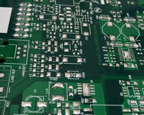
Read MoreCleanliness of bare circuit boards increases in importance with advances in PCB technology that continue to decrease conductor spacing. Inorganic contamination within printed circuit board fabrication can lead to electrochemical migration. Electrochemical migration is the dissolution and movement of metal ions in presence of electric potential, which results in the growth of dendritic structures between anode and cathode. These dendritic growths, which were minimal over periods of time, were not a concern of "yesterdays" bare boards.
Read MoreOnline quoting tools that offer customers the ability to create their own printed circuit board quotes and place orders online has become quite common in the PCB industry today.InstantPCBQuote from Epec aims to do more than the competitors. Most quoting tools are designed for lower technology parts which don't need much more than the outside dimensions of the board to provide a fast quote.
Read MorePCB Laminate Utilization - Part and Panel Size:
In our first post on controlling PCB costs, we detailed many of the common cost drivers people face and ways to avoid them. For part 2 of controlling costs, we are focusing on one example that can cost a lot of dollars: PCB laminate costs and utilization
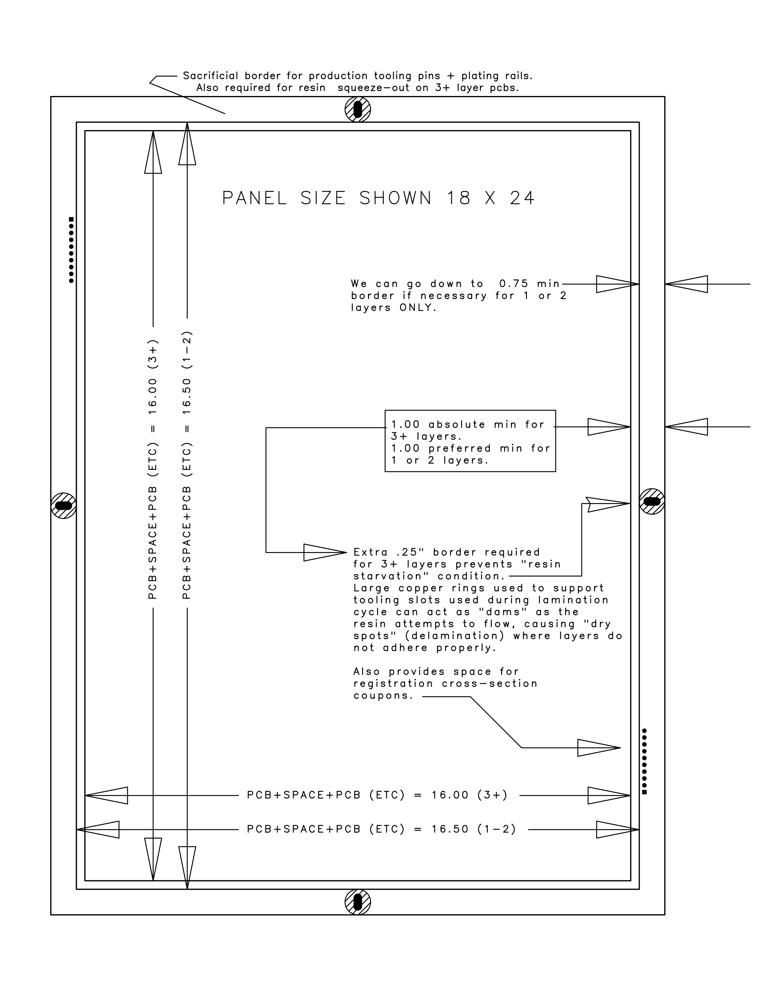
Printed circuit boards are run through the fabrication process in sheet form, typically with rows and columns of identical circuit boards or sub-panels on a single sheet, which are later cut out for shipment. One of the biggest potential cost adders in PCB manufacturing is that of a poor-yielding PCB or sub-panel. While this is true for even the least complex PCBs, it is especially true for multilayers.
Read More


