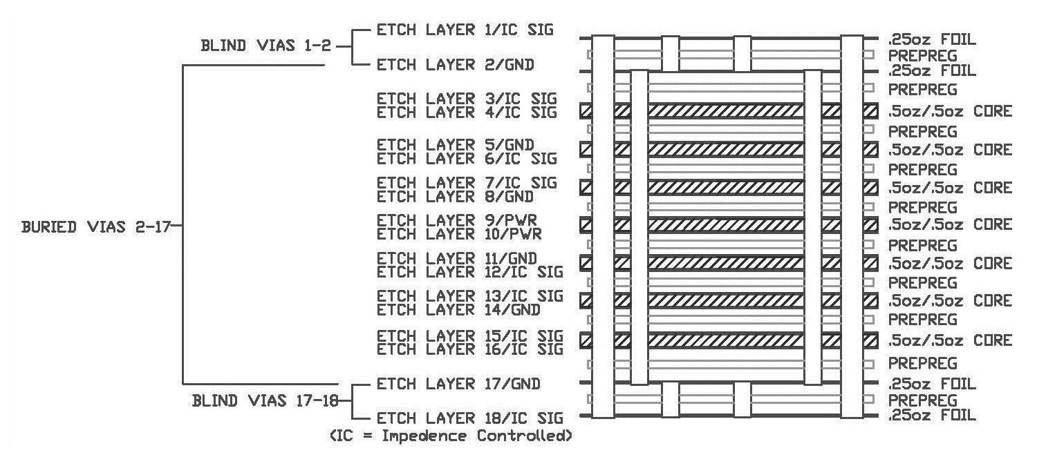
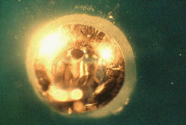
Selecting the optimal heavy copper thickness to apply to the plated through hole (PTH) plays a critical factor towards the overall reliability of the printed circuit board. There are two key elements to consider when determining optimal PCB copper thickness. The first is the current capacity of the barrel for acceptable heat rise. The second is the mechanical strength determined by the copper thickness, hole-size and whether or not there are any support vias.
Generally pads are small round or square areas of copper which are normally used to make a connection to a component pin. If these pads are not sitting correctly or are lifted, it can cause the connection between the printed circuit board (PCB) and the component to fail.
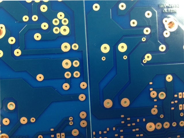
Plated through holes are the holes in a printed circuit board (PCB) with copper coated walls. These holes allow electricity to be carried from one side of the circuit board through the copper in the hole to the other side of the board. For any printed circuit board design of two or more circuitry layers, plated through holes form the electrical interconnection between the different layers.
Printed circuit boards (PCBs) with immersion finishes such as electroless nickel immersion gold (ENIG), immersion tin, silver, and OSP are appealing because they are lead-free. However, if handled improperly, these materials are susceptible to oxidation and corrosion from exposure to moisture and humidity. This oxidation causes dewetting after soldering, which can lead to poor joints at assembly and ultimately lead to failure of the board.