


Generally pads are small round or square areas of copper which are normally used to make a connection to a component pin. If these pads are not sitting correctly or are lifted, it can cause the connection between the printed circuit board (PCB) and the component to fail.

Be Careful Handling PCB!
Pad lifting on printed circuit boards during the assembly process is typically caused by a combination of a thermal and physical issue. The adhesion of the copper foil decreases as the surface heats up, so directly after soldering the copper adhesion can be low. Any handling or force applied to the components on the circuit board can cause lifting of the pads. Care needs to be taken when lifting circuit boards from the conveyor, or out of pallets, as often large components are used by operators as handles.
Although lifted pads are rarely seen on plated through-hole (PTH) circuit boards, lifting is possible. Typically this happens during the assembly stage on single-sided circuit boards. In the image below there is a lifted pad that occurred directly after wave soldering when the assembly was being handled. It’s clear to see that the solder pad has become detached from the surface of the circuit board. Overworking the joint where the adhesive bond is between copper and the circuit board may become damaged. Being cautious while handling PCBs during assembly and use of force applied to the components can help prevent the lifting of the pads.
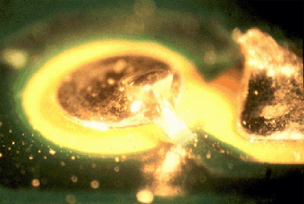
This lifted pad occurred during handling, right after wave soldering.
Feel free to learn more information on printed circuit board design and other wave soldering defects found on our website.
Summary
Pad lifting during printed circuit board (PCB) assembly is a common defect that can compromise the electrical connection between a component and the board. This issue is often caused by a mix of heat and physical stress applied after soldering, especially when the copper adhesion is temporarily weakened. Handling the board incorrectly—such as lifting it by large components—can exacerbate the problem. Although rare in plated through-hole designs, single-sided boards are more vulnerable. Proper handling procedures and awareness during and after wave soldering can significantly reduce the risk of pad lifting.
Key Takeaways
- Pad Functionality: Pads are small copper areas that connect components to the PCB. If they lift, the electrical connection can fail, impacting the performance of the board.
- Primary Cause of Pad Lifting: Heat from soldering reduces copper adhesion. If physical force is applied while the board is still hot, pads can detach from the substrate.
- Handling Risk: Pads are most vulnerable during handling right after wave soldering. Operators should avoid using components as handles when moving or lifting PCBs.
- Most Affected Board Type: Single-sided PCBs are more prone to pad lifting than plated through-hole boards, though it can still occur in both.
- Prevention Best Practices: To prevent pad lifting, allow time for cooling after soldering, handle boards with care, and avoid overworking solder joints during assembly.


