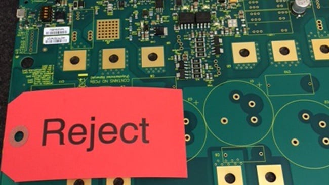
For customers and suppliers along the PCB manufacturing process, non-conformances will, unfortunately, happen from time to time. A non-conformance consists of receiving an order for printed circuit boards that do not meet your specifications or industry (IPC) standards. While dealing with these issues is obviously essential, the solution is sometimes not obvious and can put on-time delivery to your customer at risk. It is imperative that your circuit board supplier can deliver conforming product as soon as possible, which means having the procedures to get there.
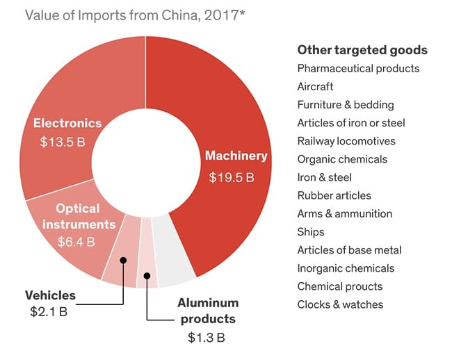
Read MoreTariffs and trade with China has been a hot topic in the news recently. The tariffs impacting the steel and automobile industries have been widely covered but there are many additional industries that could potentially feel the effects of these tariffs, including our own.
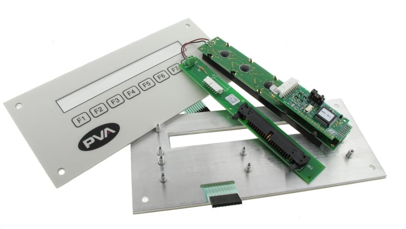
Read MoreAs capacitive touch human machine interface (HMI) assemblies become more popular, both designers and users are becoming more familiar with the technology as it replaces traditional mechanical HMI products. These capacitive touch HMIs can be used in extreme environments, with users wearing gloves, and can operate reliably for years.
Just as a mechanical HMI (membrane switches, tactile switches, etc.) relies on the overlay material properties to determine system function, capacitive touch HMIs rely on the overlay material properties to drive capacitive touch sensitivity and overall system performance.
Read MoreWhen our customers are in the preliminary stages of launching a new SMART HMI project, they typically reach out seeking advice on the best way to start. With what can amount to a near infinite number of HMI design options and system feature combinations, brainstorming an embedded firmware project can quickly become overwhelming. Where does one begin? How does the firmware work? What level of detail is required now?
Read More“The power of the Internet of Things comes from the ability to collect a lot of data and convert that into useful information.” ~Bertil Thorvaldson, ABB Robotics
While that is a very simple concept to understand, manufacturing Internet of Things (IoT) technology into most products can be a significant investment of time and money for companies. As a designer and manufacturer of medical, commercial, industrial, and military products, we are working with many customers on implementing IoT into their products to improve the customer experience and provide an additional revenue stream.
Read MoreWith the introduction of ISO 9001:2015, which specifies requirements for quality management systems, the statement “quality management system documentation shall include a quality manual” no longer need apply. Many celebrated this as a reprieve from previously having to fully document their quality management system. However, eliminating the supplier quality manual altogether could be a dangerous takeaway on the new standard’s intention.
Read MoreIn front-end engineering, we must gather as much manufacturing information as possible from the printed circuit board data we receive. This includes customer service notes, customer emails, and the general spec, if available. Usually there is enough information to release a printed circuit board (PCB) package to manufacturing. However, I have found many gray areas that haunt our engineering department.
Read MoreAs today’s printed circuit boards (PCBs) become smaller, they use fewer and fewer through hole components. It is increasingly difficult to justify allocating precious space for relatively large plated through component holes and their accompanying lands. Instead, it is necessary to use surface mounted components wherever possible. As surface mount technology becomes increasingly prevalent, the majority of the plated through holes on most modern PCB designs end up being vias.
Read MoreAmong the most common questions printed circuit board suppliers receive are those dealing with production capabilities. Customers often suspect that they are about to design-in a feature which may be either at or outside their fabricator’s limits. Fearing that their non-standard feature may add cost to their product, they inquire to find out just how much pain they are about to cause.
Read MoreWhen it comes to manufacturing custom electronics, there are tons of companies out there that can do anything once. The true value of a manufacturing partner is a company that not only has the capability to manufacture your product fast to help you get to market quicker and cost effectively, but also consistently. Effectively accounting for Engineering Change Orders (ECOs) and product changes are factors that often get overlooked in manufacturers. Failing to find a supplier with stable speeds, costs, and a consistent process can cause major headaches down the line.
Read More


