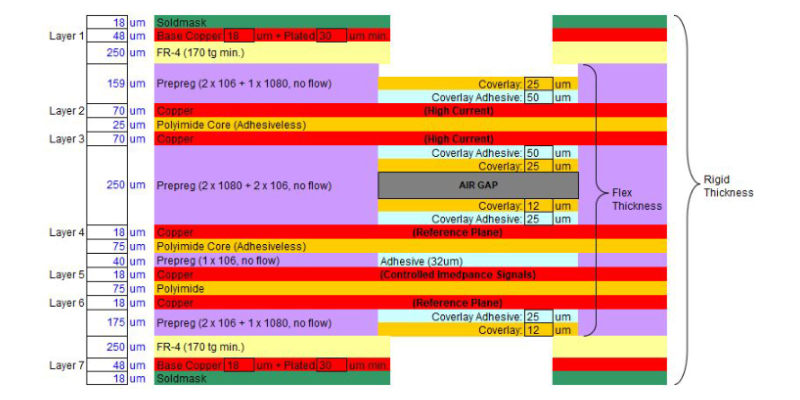
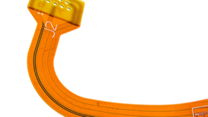
Higher current carrying flex circuit designs create challenges that need to be addressed early in the design process to ensure both a manufacturable design and that it will reliably meet the bend requirements. These items range from material types/availability, bend capability/flexibility, impact on standard signal lines, and part cost.
Read MoreAt the conclusion of our webinar, How PCB Design Choices Affect Overall Cost from Your PCB Fabricator, we had several questions submitted to our presenter, Ed McMahon, CEO at Epec. We have compiled these questions into a readable format on our blog.
Read MoreAt the conclusion of our webinar, Using Rigid-Flex PCBs to Improve Design Reliability, we had several questions submitted to our presenter, Product Manager of Flex & Rigid-Flex Circuits, Paul Tome. We compiled these into a readable format on our blog.
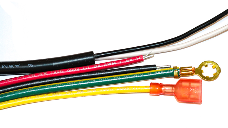
Read MoreOne of the first steps in designing a custom cable assembly is selecting the wire. There are lots of options to choose before the design can be frozen. Selecting a UL spec wire can be challenging if you are unfamiliar with the standards but knowing just a few options allows for a simplified design.
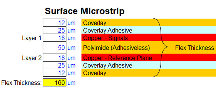
Read MoreFlex and rigid-flex circuit boards are a combination of both electrical and mechanical requirements that allow for solutions to many tight packaging requirements. However, this combination is also the potential source of design challenges as some electrical requirements can have a negative impact on the mechanical bend capabilities of flex circuits. If not, correctly addressed the reliability of the finished design may be compromised.
Read MoreDynamic flexible circuit boards have the capability of solving many interconnect and packaging challenges in designs that require repetitive motion. They allow for extremely high-density interconnects while consuming a very small amount of space. However, these applications have a different set of design rules than that of a “one-time” or “bend-to-fit” static application.
Read MoreAt the conclusion of our webinar – Design Considerations for Lithium Batteries Used in Portable Devices – we had several questions submitted to our presenter, Battery Development Consultant Randy Ibrahim. We compiled these into a readable format on our blog.
Read MoreAt Epec, engineers are expected to find innovative solutions to problems and develop them quickly and accurately so that customers can get quality products delivered on time. In this blog post, I will discuss how the 80-20 rule can be used in conjunction with our classic engineering design process to reach solutions faster.
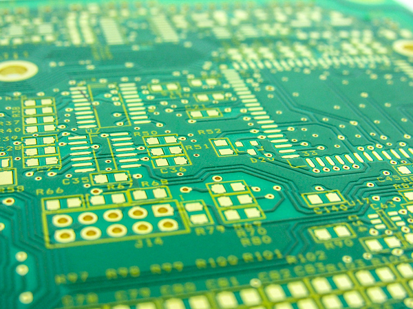
Read MoreAt the conclusion of our recent webinar – Match Your High-Tech PCB Design To Your Supplies Capabilities – we had a number of questions for our presenter, PCB Field Applications Engineer Al Wright. We decided to compile these into a readable format on our blog.
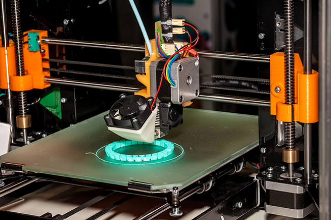
Read MoreAt Epec we work on such a varied and technical catalog of products, so our engineers must be comfortable leveraging every manufacturing technology available to them in order to create solutions in design and production. One of the most important technologies that we use is 3D printing.
Read More


