For every flexible circuit board manufacturer, there are some key areas you should be aware of. While flex circuits have some similar characteristics to rigid printed circuit boards, they require very different approaches in the manufacturing process.
Some of the more significant areas are:
- Thin Material Handling Capabilities and Procedures
- Selective Pad Plating
- Polyimide Coverlay Manufacturing
- Material Dimensional Tolerances
- Laser Profile Cutting
- Plasma Desmear and Etch Back
Thin Material Handling Capabilities and Procedures
Material handling, during the flexible PCB manufacturing process, is critical to achieving a high production part yield rate and reliable finished circuits. Handling can account for the largest percentage of production scrap and reliability issues. Flex materials are much thinner and not reinforced than those used in rigid boards. Flex core materials are typically 1-3 mils thick with either ½ oz. or 1 oz. copper and Coverlays are 1.5–2 mils thick.
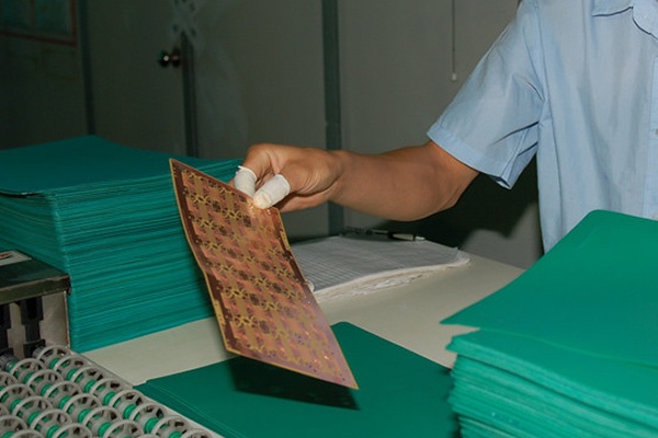
Material Handling During Flex PCB Manufacturing
These thin materials require a lot of the process equipment to be specifically designed to transport the flex materials safely and without damage. Employees must also be trained in well-defined manual handling methods. Any kinks or creases in a production panel will either result in scrapped parts or reliability issues in the finished circuits.
Selective Pad Plating
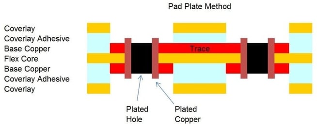
An important manufacturing technique is how and where copper is plated on the parts. Flex circuits require a Pad Plate method which limits plated copper to within the holes and to a small circular area surrounding the holes on the surface of the part. Additional copper is not plated on the surface of any traces. For high density designs, the circular area on the surface may need to be planarized away to allow for effective pad and trace imaging.
Any plated copper on the traces of a flex circuit will decrease the flexibility of the part and potentially compromise its mechanical bend reliability resulting in breakage.
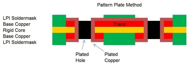
Rigid PCBS utilize a Pattern Plate method which plates additional copper on the surface of all the external traces.
Flex Circuit designs may also require review to ensure that any current carrying requirements are being met by the thickness of the base copper alone.
Polyimide Coverlay Manufacturing
Coverlays serve the same purpose of Soldermask on rigid boards but are solid sheets of Polyimide with an adhesive backing that require a completely different manufacturing method. All required openings to expose the SMT and PTH pads, must be machined in some manner using laser cutting, drilling / routing, CNC knife cutting, punch and die sets, or a combination thereof. Coverlays are then positioned and laminated under heat and pressure to the surfaces of the part. The machining requirements also mandate a different set of rules governing feature size, shape, configuration, and positional tolerance.
Material Dimensional Tolerances
Due to the required flexibility, flex materials are much thinner and contain no reinforcement (i.e. glass weave in rigid boards). This results in much less dimensional stability in the materials which needs to be accounted for in the tooling/registration systems used in manufacturing. Flex materials will grow and shrink as they are subjected to moisture, heat, and pressure as seen throughout production.
It is also common practice to use smaller production panel sizes than rigid boards to mitigate the impact of the material dimensional stability.
Laser Profile Cutting
Polyimide materials are easily cut with a laser. This allows for very accurate and complex profile It also eliminates the need for costly hard punch and die tooling at prototype and lower production volumes. Routing can be used but can limit the complexity of the profile and results in an undesirable ragged part edge. Laser cutting will leave a small amount of carbon residue on the part edge but has been deemed acceptable by IPC standards.
Plasma Desmear and Etch Back
Multilayer flex designs require an effective desmear and etch back process which is critical to ensuring reliable plated holes and inner layer interconnects.
The material properties of Polyimide and flex adhesive, used to laminate layers together, are substantially different from that of rigid board materials. Common chemical based etch back processes used on rigid boards are far too aggressive. This results in a very small and difficult to control process window, inconsistent results and reliability issues on finished parts. Plasma based etch back is overwhelmingly preferred, which results in high quality and consistent results.
Summary
As mentioned in the beginning of this post, from a design standpoint, you need to be aware of some key areas to manufacture flexible PCBs. Not only should you be aware of the design aspect, but you should also take into consideration who will be manufacturing your parts. When selecting an offshore flex PCB manufacturer there are some additional checks and balances you should looks into as well.
Key Takeaways
- Thin material handling is critical: Flex cores and coverlays are only a few mils thick, requiring specialized equipment and strict manual handling methods to prevent creasing, scrap, and reliability failures.
- Selective pad plating protects flexibility: Unlike rigid PCBs, flex circuits use pad plating rather than pattern plating to avoid adding copper to traces, which could reduce bend reliability and cause mechanical breakage.
- Polyimide coverlays replace soldermask: Openings must be precisely machined by laser, CNC, or drilling, and then laminated, with unique rules for feature size, tolerance, and placement.
- Dimensional stability is a challenge: Flex materials expand and contract with moisture, heat, and pressure. Smaller panel sizes and specialized registration systems are required to maintain accuracy.
- Advanced processing ensures reliability: Laser profile cutting enables precise shapes without costly tooling, while plasma desmear and etch back deliver consistent plated holes and interconnects, outperforming aggressive chemical methods.


