In 1999 there were over 1,200 active printed circuit board (PCB) manufacturing facilities in the U.S. Today, there are fewer than 130. What has transpired at a lot of these manufacturing companies are small service businesses that act as a liaison between a manufacturer and their customers. In many instances, this is a valuable relationship; the products are low in technology and the risk is very minimal. However, why is it that we require certification to ISO standards for our manufacturing locations but not for service providers?
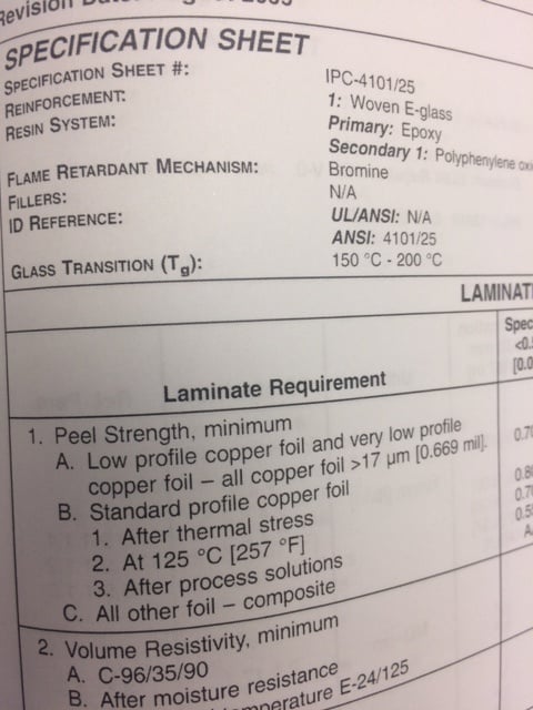
Read MoreIPC 4101 (Specification for Base Materials for Rigid and Multi-Layer Printed Circuit Boards) was released for publication in December, 1997. It was released as the replacement standard for MIL-S-13949. However, it contained a majority of the exact wording from the military standard. It maintained the “slash sheet” format appendix to the standard that specifies the resin and fiber system of different PCB laminates, along with testing parameters and properties. Initially there were 41 slash sheets, but as the industry opens up to “Lead Free” and “Green” processes, the slash sheets have increased to 66, the current revision.
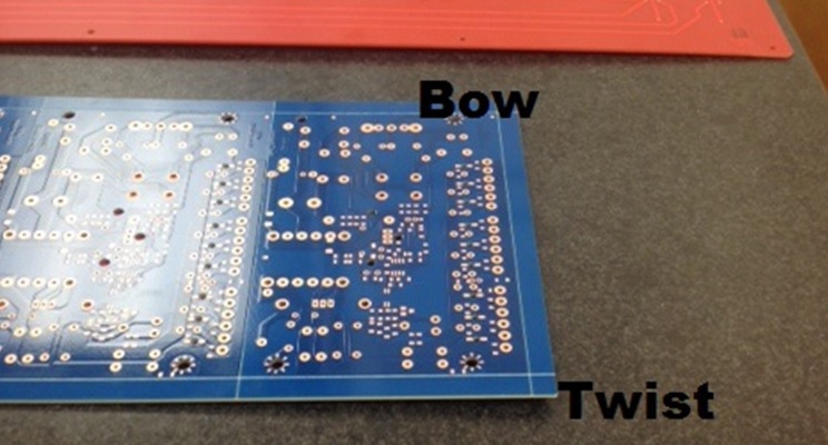
Read MoreBow and twist of printed circuit boards (PCB) routinely rank among the highest levels of falsely identified non-conformance because it is perhaps the least understood. Envisioning a perfectly flat rigid circuit board as the standard is a fallacy believed by many incoming inspectors. Understanding the reasons and causes for PCB bow and twist can help resolve the issue at the board design stage.
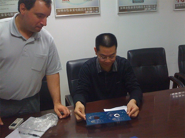
Read MoreThere was a time when “Made in China” was synonymous with cheaper, poor quality products. "Buyer beware" was the common theme associated with outsourcing to any Asian PCB manufacturers. So how did Epec approach this challenge and succeed? It was by managing quality through intense auditing, training, and qualification. Epec understood at a very early stage that first-class quality products from Asian manufacturers would require consistent presence, training, and auditing.
Read MoreCleanliness of bare circuit boards increases in importance with advances in PCB technology that continue to decrease conductor spacing. Inorganic contamination within printed circuit board fabrication can lead to electrochemical migration. Electrochemical migration is the dissolution and movement of metal ions in presence of electric potential, which results in the growth of dendritic structures between anode and cathode. These dendritic growths, which were minimal over periods of time, were not a concern of "yesterdays" bare boards.
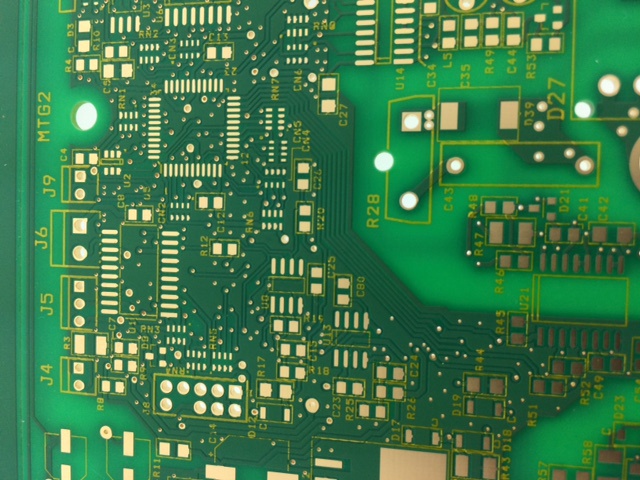
Read MoreWhen creating your optimal circuit board design, one factor that must be considered is the solder mask and whether to go with matte finish solder mask or gloss finish mask for your final product. Usually, most designers don't specify their preference and end up leaving the decision to the PCB fabricator. Most fabricators will likely default to a gloss surface finish, the more popular choice of the two.
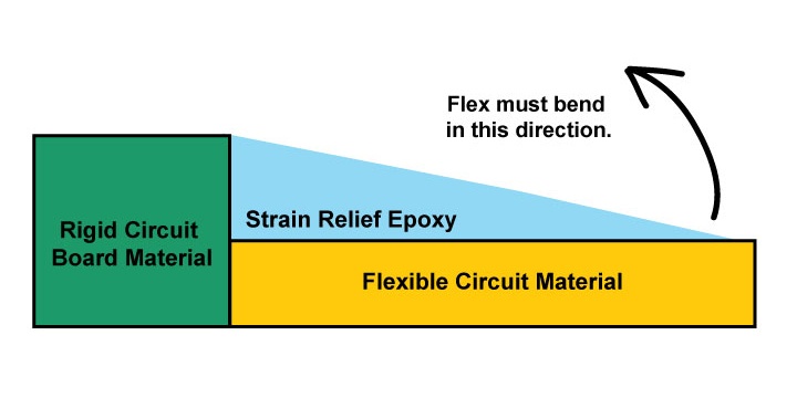
Read MoreFor rigid-flex printed circuit boards (PCBs), the space joining rigid material to flex material (Transition Zone) sometimes contains imperfections that, although acceptable, could impact effectiveness of the final part. Transition zone imperfections can include any of the following:
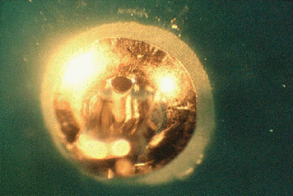
Read MoreWhen a blow hole defect occurs during the assembly process as a result of the PCB card, the primary culprit tends to be entrapped moisture or air. With moisture, any non-plated and non-masked areas on a bare circuit board that expose internal laminate can be suspect to absorbing moisture. Absorption can occur either during the board fabrication process or from improper storage. Examples of highly suspect areas include non-plated drilled holes and routed features.
Read MoreIt is not recommended to bake boards with an organic solderability preserve (OSP) surface finish. Although baking a printed circuit board with an organic solderability preserve finish can have negative consequences, the process itself can have positive performance in specific applications. OSP is a very thin protective layer of material placed over exposed copper, typically using a conveyorized process to protect the copper from tarnish.
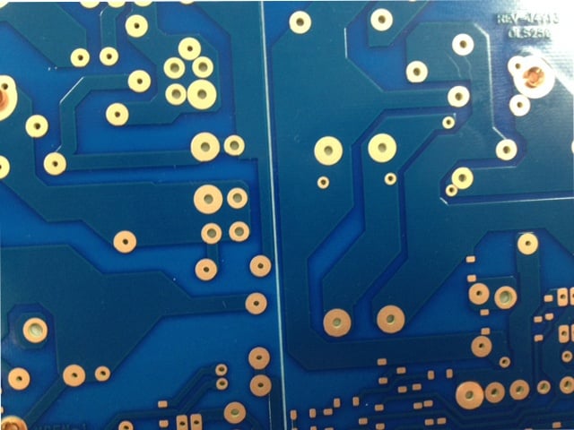
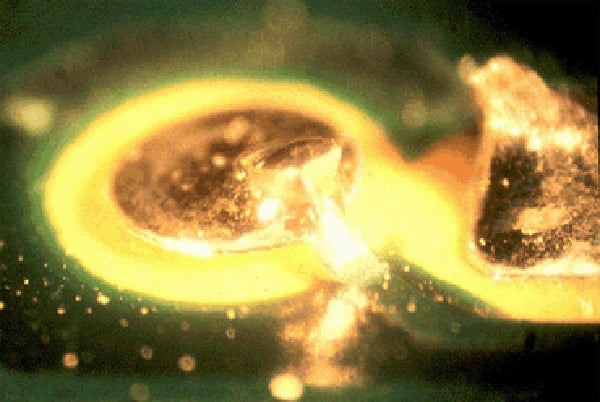
Read MoreGenerally pads are small round or square areas of copper which are normally used to make a connection to a component pin. If these pads are not sitting correctly or are lifted, it can cause the connection between the printed circuit board (PCB) and the component to fail.
Read More


