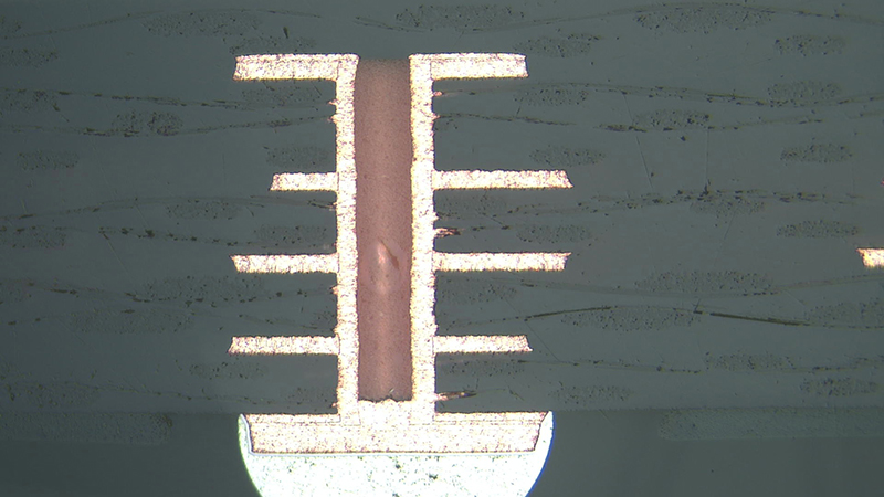
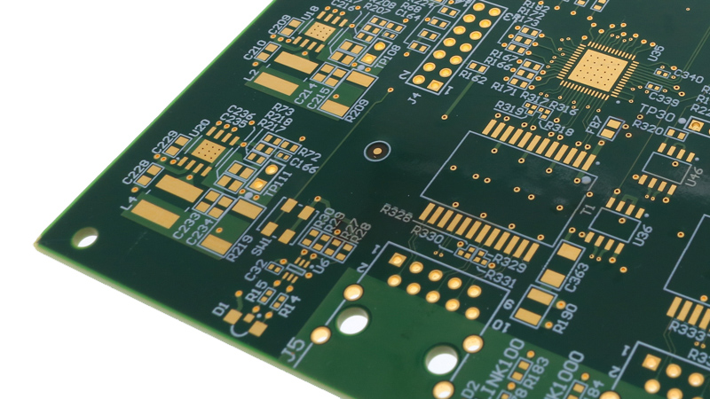
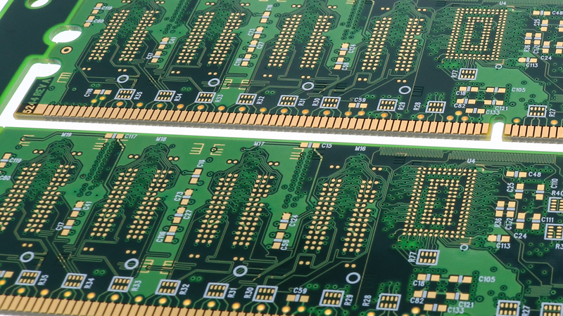
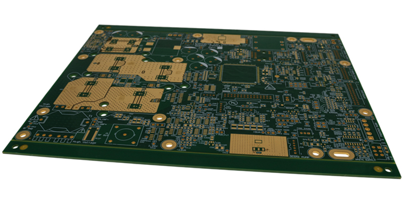
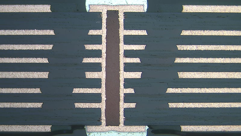
Wrap plating is a technique used in the manufacturing of printed circuit boards (PCBs) to create a conductive layer that connects the layers of the PCB together. The process involves plating copper onto the walls of through-holes and vias in the PCB, which are then used to make electrical connections between the layers.
Read MoreAs I think about the processing of multi-layered printed circuit boards (PCBs), I find it interesting that in the early 1980s, I wouldn’t have dreamed of where we are today in terms of technology. I mean, think about it. Where we are in comparison to then is simply phenomenal.
Read MoreYou may be asking: what is an HDI printed circuit board and what makes it different than standard PCBs? Let’s break it down for better understanding from a design and from a supplier point of view. As Epec continues to grow our design business, it has become very apparent that many designers are very good at what they do and have no manufacturing knowledge to proof designs against.
Read MoreMore often than not, a quote will be requested without enough information to price, never mind to manufacture. In 1957, IPC was founded as the Institute for Printed Circuits by Richard Zens (Printed Electronics Corp/Epec), Al Hughes (Electralab), Robert Swiggett (Photocircuits), William McGinley (Methode), and Carl Clayton (Tingstol).
Read MoreEtch compensation is a process used in the design of printed circuit boards (PCBs) to adjust the trace widths to compensate for any changes that occur during the PCB manufacturing process. When PCBs are manufactured, the etching process used to create the copper traces on the board can cause some amount of variation in the width of the traces. This variation can be caused by factors such as the thickness of the copper, the quality of the etching process, and the chemical composition of the etchant.
Read MoreIn printed circuit board (PCB) designs, through holes are used to connect components and conductors on different layers of the board and can be divided into two types: plated and non-plated through holes.
Read MoreI am still amazed at how far technology has brought us throughout the years. When asked about printed circuit boards (PCBs) and what they go into, the answer is everything you can imagine, everything you use in most cases.
Read MoreAt the conclusion of our webinar, PCB Manufacturing Facilities: Certifications, Compliance, and Security - we had several questions submitted to our presenter, Ed McMahon, CEO at Epec. We have compiled these questions into a readable format on our blog.
Read MoreAs the oldest production printed circuit board (PCB) company in North America, perhaps in the world, the 70+ year story of Epec Engineered Technologies is connected to the development of the PCB and the electronics industry. Epec’s storied history also includes delivering PCBs for the Apollo 11 spaceflight.
Read MoreSo, let’s talk about non-recurring charges, better known as NREs, that are applied to most new and new revision first-time orders for manufacturing of printed circuit boards (PCBs). These charges help aid in several crucial steps for manufacturing with a cost of processing, programming, testing, and manpower to deliver a quality product.
Read More


