


During the manufacturing of printed circuit boards (PCBs), a lot of attention is focused on how tools and processes are handled to avoid many common quality issues such as brittle joints, cold joints, and voids. Voids consist of an empty space somewhere along the PCB where not enough of a certain material was added. If the voiding issue is not addressed, then the entire PCB may need to be scrapped.
To help our customers avoid this common issue and all the additional problems that it creates, we'll explore everything you need to know about PCB voids and how to avoid them, including the two most common types of voids, the issues that they cause during the PCB manufacturing process, and the measures that you can take to avoid PCB voids.

What Are PCB Voids?
PCB voids occur anytime there is an un-plated area in the circuit board - either within the hole wall of the PCB drilled plated hole, within hole barrels, or within a solder joint. These voids can disrupt the electrical connections within the circuit, leading to malfunctions.
There are two main types of PCB voids: plating voids and solder voids. Plating voids happen during the electroless copper process when the copper plating does not completely cover the inner walls of the through-hole. Solder voids happen when not enough solder paste is used or when air pockets occur when the solder paste is heated as the air does not escape. In both cases, these voids can render a circuit board inoperable and leave manufacturers with no other option but to scrap it.
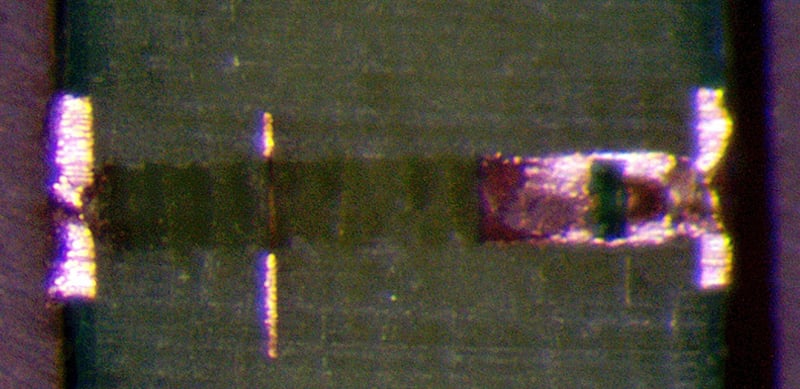
Example of copper plated void during PCB manufacturing.
Plating Voids
Plating voids typically occur due to the drilling process and how it may prepare the through-hole. If a worker uses a dull drill bit, the bit may leave imperfections along the wall instead of a smoother surface. These imperfections may cause the hole wall to be rough and have inner imperfections. When the copper plating is added during the electroless copper process, the copper simply cannot get into every rough spot or crevice in the hole, leaving a non-plated spot.
Another way that plating voids occur is when debris becomes lodged inside the hole. This debris may come from when the worker removes the drill bit, yet the hole is not cleaned out well enough. When the copper enters the hole, it may cover over the debris and other contaminants. However, the debris may later become dislodged from inside the hole, leaving a bare spot that was not plated. The debris inside the hole may cause the copper to create a void as the copper cannot adhere properly to the surface walls of the hole.
Additionally, entrapped air bubbles in the electroless process can prevent copper solution from contacting the barrel wall, thus causing a void.
Solder Voids
A solder void is generated when there are empty spaces within a solder joint. There are a number of factors that can lead to this issue, including a low preheat temperature that prevents the solvent in the flux from vaporizing completely, high levels of flux, solder paste oxidization or using low-quality solder paste, and the design of the PCB itself since some circuit board designs are more prone to voiding than others.
The good news, though, is that solder voids are typically easier to prevent than plating voids. Extending your preheat time, avoiding low-quality and outdated solder paste, and modifying your circuit board stencil are all effective ways to mitigate the risk of solder voids.
PCB Problems Caused by Voids
Solder voids and plating voids alike can create a number of issues during the PCB manufacturing process, the biggest issue being a loss of conductivity.
In a PCB, the plating within the holes is used to connect each conductive layer of the circuit board between the layers and from the top to the bottom of the board. The PCB becomes powered by these electrical connections. When there is a void or un-plated area, though, the electrical connection can become disrupted, causing the current to not flow properly. These issues may lead to the PCB malfunctioning or signals not reaching designated areas of the circuit board's components.
When dealing with voids or plating voids, the PCB may have to become scrapped due to failing inspection. For some applications, having just a few voids may allow it to pass the testing. In other cases, though, even a single void can render a circuit board inoperable. For this reason, preventing voids is a key objective in the PCB manufacturing process.
Avoiding Plating Void Issues
The best way to prevent void issues will be based on the types of voids that have commonly occurred during PCB manufacturing processes. To avoid plating issues, manufacturers need to take proactive steps to address how drilling and hole cleaning is conducted.
Drilling too fast, for example, can cause the drill bit to shatter the circuit board's material on the way down, leading to rough and uneven surfaces difficult to coat evenly during deposition and plating. Likewise, using a drill bit that is dull and worn can once again yield uneven surfaces that make plating voids difficult to avoid.
To prevent voids created by the drilling process, drill bits should be sharpened or discarded based on hit count records, drill speeds, and drill feeds. Following cleaning procedures for every drilled hole, proper racking, and controlling as well as monitoring bath plating agitation with the tanks may also help to reduce and eliminate plating voids.
Entrapped air during the electroless process can be avoided with line vibration and angles plating racks.
Summary
Manufacturing printed circuit boards can become a costly process when dealing with PCB scrapping due to plating voids. Thankfully, a little precaution and extra attention to detail can prevent most PCB voids.
Having established drilling and cleaning procedures, as well as extensive testing, can reduce void occurrences and ensure high PCB quality. Manufacturing design review between the manufacturer and customer can also help save on costs and ensure a smooth production process for PCBs. By following these tips for PCB void prevention, you can help prevent one of the most common causes of PCB malfunctions.
Key Takeaways
- Plating and Solder Voids Disrupt PCB Functionality: Voids are empty areas where plating or solder is missing, typically due to rough drilling, trapped debris, or flux issues, and can interrupt electrical connections, potentially rendering the board inoperable.
- Plating Voids Originate from Poor Drilling or Cleaning: Dull drill bits, high drill speeds, or leftover debris in through-holes can lead to rough walls or blockages that prevent proper copper adhesion during electroless plating, resulting in plating voids.
- Solder Voids Are Often Easier to Prevent: Common causes include insufficient preheat, oxidized or low-quality solder paste, and poor stencil design. These can be addressed by adjusting reflow profiles and improving paste quality.
- Voids Can Lead to PCB Scrap or Failure: Whether due to interrupted conductivity or failing inspection standards, voids, especially plating voids, often result in costly board rejections and lost production time.
- Prevention Requires Process Control and Maintenance: Avoiding voids depends on strict control over drilling, cleaning, and plating procedures. Regular maintenance of equipment, bath agitation, and design collaboration between OEM and fabricator help ensure void-free boards.


