


Printed circuit boards (PCBs) require holes to be drilled through or partially through laminate materials. These holes are used to create continuity between the top and bottom or to a mid-layer on the PCB. The holes allow traces, pads, and copper polygons to be connected throughout the different layers of the board.
Mechanical drilling and laser drilling are two methods that can create the drilled holes in the PCBs. There are advantages and disadvantages to each method, as well as considerations to consider when deciding on the depth of the hole, the diameter, and when back drilling needs to be performed.

Mechanical Drilling: Pros and Cons
Mechanical drilling relies on a rotating bit tool to cut through the different types of laminate materials. The bit is typically made from a micro-grain carbide, allowing the drill to be used for many repetitions. They can also be resharpened for reuse with a maximum number of times of three usually. The standard laminate is made of a fiberglass and resin content with a copper foil covering the substrate is commonly known as FR4.
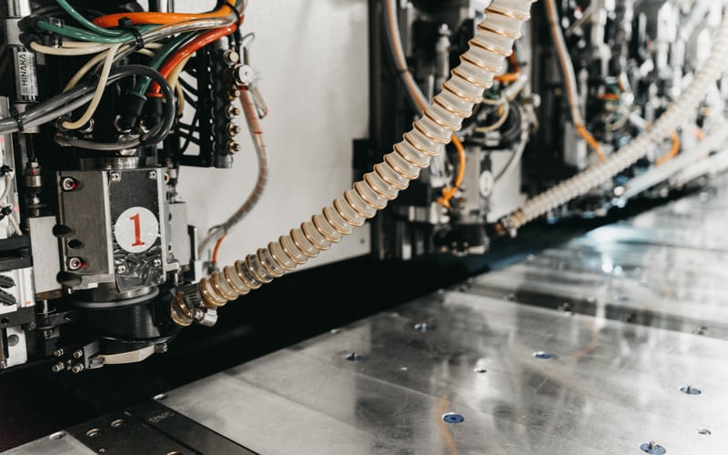
Example of mechanical drilling machines used in PCB manufacturing.
One advantage to using mechanical drilling is that the tool creates very high-quality holes that are consistent in nature no matter the number of holes that are drilled. The holes do not have a taper at the ends, they are drilled through the substrate completely leaving the knee of the wall clean with no bevel; the surface edge has a sharp finish. Another advantage is that mechanical drilling has a faster drill speed than other methods, allowing for increased throughput for production quantities.
A disadvantage to mechanical drilling involves the size of the bit that must drill through the multiple layers of the materials used for the printed circuit board and the size of the hole. If requiring exceedingly small hole sizes, such as microvias less than 0.008 mil. diameter, with higher trace densities, a thinner bit tool may break during the drilling process. While mechanical drilling is a faster method than laser drilling, each hole will need to be deburred. Burrs are elevated ends of copper that may be left during the drilling process. Deburring removes these pieces of copper. Depending on how complex the circuit board is, and the number of holes required, the process can take a longer time than wanted based on deadline schedules.
Mechanical drilling is an expensive, time-consuming process. The drills are prepped for processing, drill selection, and setup time can take many minutes. The time to drill the PCBs can also be many minutes to over hours long. Hand selection of the proper tools by humans leaves this process vulnerable to errors. The wrong drill used will cause scrap and a costly restart.
Laser Drilling: Pros and Cons
Laser drilling relies on a stationary machine that uses a high-density laser beam to ablate a hole into the PCB. The same materials are used in this process as in standard mechanical drilling. There are various types of lasers used depending on the type of material being cut; the two most common are UV and CO2.
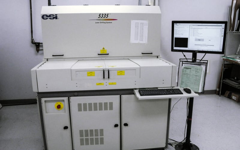
Example of laser drilling machine used in PCB manufacturing.
Advantagesto laser drilling consists of the laser being able to ablate through a wide range of materials using a wide variety of diameters and radii not available through conventional mechanical drilling. In addition, a large quantity of holes can be drilled into the single PCB as it can provide a higher manufacturing speed depending on the quality of the holes. Laser drilling is also a non-contact technique. It requires less handling than when using mechanical drilling and tool selection as a manual process.
There are several disadvantages to the laser drilling process. It can be difficult to get accurate depth control if there is not a metal stop layer, and tapering can result when the depth-to-width ratio is large. A disadvantage would be that it carbonizes the edges that it cuts, which usually leaves are dark or burnt appearance.
Considerations When Deciding Between Mechanical and Laser Drilling
Size of the Vias
The size of the holes and the pad-to-hole ratio is the determining factor when deciding the method of drilling. The drilling has to take two key factors into consideration: pad-to-holes ratio and the aspect ratio.
Pad-to-hole ratios are often not considered during the design phase as related to the PCB process. All holes ideally are drilled on center of the conjoining pad. The desired hole size, for example 0.010” +\-0.003” in diameter is considered to be a via hole. The small diameter indicates this hole is strictly for passing current from layer to layer and will not be used for insertion of a component. In this case, the hole size bottom tolerance of -0.003” could be less the hole size and still function as needed. The minimum copper pad size for annular ring with no break allowed should be 0.015” greater than the desired hole finished size. For 0.010” hole a 0.025” copper pad would allow for a 0.015” hole to be drilled, plated and final plate surface finish to finish at 0.010” +\- 0.003”.
For another example: 0.028” finished component hole used at assembly for insertion would be drilled with an 0.033” drill size to allow for plating and surface finish applied and to maintain annular ring therefore the pad size should be a minimum of 0.043” diameter. Understanding the upsizing of the drill is the critical point to be made, a desired hole needs 0.005” increased room for processing in production.
The aspect ratio is determined by the overall thickness of the printed circuit board during primary drilling without plating applied and the diameter of the smallest drilled hole. The holes are drilled from the top to the bottom through the PCB. To determine the aspect ratio, take the overall thickness and divide that number by the smallest diameter hole.
For example: 0.093” thick PCB divided by 0.010” via hole is a 9:1 aspect ratio; 0.062” thick PCB with 0.007” diameter hole is an 8:1.
The larger the aspect ratio is, the more difficult the plating process becomes. A simple rule of thumb is thicker boards need larger vias. Longer plating time and processing can increase the chances of cracks in the hole wall due to expansion. The lower aspect ratio has stronger bonded hole walls and less chance of cracking.
Blind and Buried Vias
Unlike through drilling where you use a mechanical bit or a laser to go through the entire PCB, there are times when the via will only pass through a few layers of the PCB. These processes are called blind vias and buried vias. A blind via will connect the exterior layer to the interior layer of the PCB. A buried via will connect two inner layers together. Blind and buried vias are typically done to multilayer PCBs. Through vias, connecting one exterior layer to the other exterior layer, usually are reserved for simple 2-layer boards.
Both mechanical and laser drilling can perform blind and buried vias. However, keep in mind that laser drilling has less depth accuracy and may cause tapering along the edges of the hole. An etching step is also often used to help the laser cut through the layers, and care must be taken to ensure the laser does not ablate through the copper pad.
When drilling through holes using mechanical, sometimes part of the barrel of copper needs to be removed to create sort of a blind hole. Removing the copper from the barrel partially either from the top or the bottom is called back drilling. Back drilling is used to remove as much of the barrel as needed but keeping the continuity where required. Back drilling involves using a drill bit in a larger size to remove all copper.
Summary
Mechanical drilling and laser drilling both offer their advantages and disadvantages in circuit board manufacturing. Your PCB supplier will decide the methods needed during the engineering review to successfully process your order. Knowing the process to manufacture a PCB at the design level is advantageous to the ease of processing.
Key Takeaways
- Mechanical drilling delivers clean, high-quality holes with consistency: It's ideal for standard via sizes and thick PCBs, offering sharp-edged holes and strong barrel walls. However, it's slower, more labor-intensive, and less suited for microvias under 0.008".
- Laser drilling is preferred for microvias and complex multilayer designs: Lasers provide precise, small-diameter holes with less manual setup and better speed for high-density designs, but with challenges like tapering and edge carbonization.
- Pad-to-hole ratio and aspect ratio dictate the drill method: The minimum annular ring and proper aspect ratios are critical for manufacturability. High aspect ratios (over 8:1) increase plating complexity and the risk of via cracking.
- Blind and buried vias add design flexibility but increase process complexity: Both mechanical and laser drilling can be used, but depth control is crucial, especially for blind vias. Laser drilling may require extra etching steps to avoid damaging copper layers.
- Back drilling is a mechanical technique to remove unused via stubs: This process helps reduce signal reflections in high-speed boards, improving performance while retaining required electrical paths between specific layers.


