


Advancing technology has impacted rigid-flex PCB designs in the same manner as rigid printed circuit boards. Increasing interconnect requirements and smaller form factors require higher circuit densities and increased layer counts. The impact of these elements on rigid-flex circuit designs is potential reliability issues both electrically and mechanically.
In this blog, we discuss the specifics of both the electrical and mechanical concerns and how to eliminate them by utilizing an air-gap design and construction method in your rigid-flex PCB.

 .
.
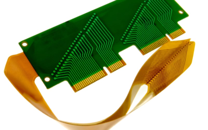
Rigid-flex PCB with air gap construction.
Impact of Higher Flex Layer Counts
The typical method of addressing higher layer counts in a design is to laminate them into one finished structure. This works for rigid circuit boards but creates both electrical and mechanical reliability concerns in a rigid-flex circuit board design.
The first issue is mechanical bend capability. The thicker a flex area, the less the bend capability due to the added strain placed on the copper circuitry. A common minimum bend guideline for a 1- to 2-layer flex, in a static application, is 10X the flex thickness. This increases to 20-30X for a laminated 4-layer flex section. If the minimum bend capability is exceeded, the circuitry may crack, creating either complete or intermittent open circuits. A manufacturer is incapable of modifying the physical properties of the materials. This can only be addressed through design and construction methods.
The second issue of electrical reliability stems from the materials used in a rigid-flex PCB construction. Beyond the FR4 based rigid and pre-preg layers, used in the rigid areas, flex layers are laminated together using either a flexible acrylic or epoxy-based adhesive. Given that the flex layers extend throughout the rigid areas, so do the lamination adhesives. A negative property of both is that they have a much high co-efficient of thermal expansion than either FR4 or polyimide materials. When the rigid-flex circuit board is assembled or long term as the temperature fluctuates on the finished assembly in the field the adhesives expand and contract and place vertical stress on the via hole plating. This can also result in the formation of cracks in the copper plating and either complete or intermittently open circuits.
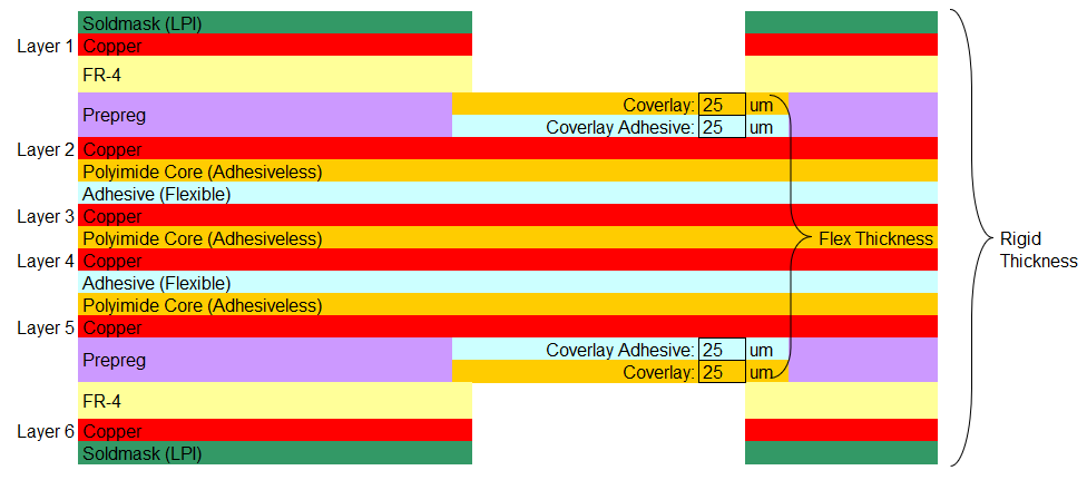
Example of a 6-layer rigid-flex PCB stack-up with 4 laminated flex layers.
Air Gap Rigid-Flex PCB Design & Construction
To address the above concerns the industry, combined with IPC, developed a design and construction method referred to as an air-gap construction. In this configuration, the flex layers are retained as multiple individual sets, containing no more than 3 layers per set, as opposed to one lamination containing all layers. The preferred configuration is 2 layers per set, but IPC 2223 does allow for 3 layers if a design has controlled impedance lines in the flex area that has to be configured as a stripline for 2-sided shielding purposes. A surface microstrip configuration in the flex layers requires only 2 layers. The most common design configuration has 2 sets of flex layers, but it can have more. Note that a higher number of flex layers sets will ultimately constrain the bend requirements.
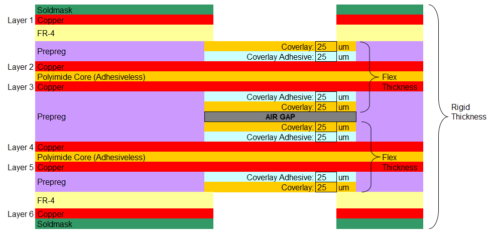
Example of a 6-layer rigid-flex PCB stack-up with 4 air-gap flex layers.
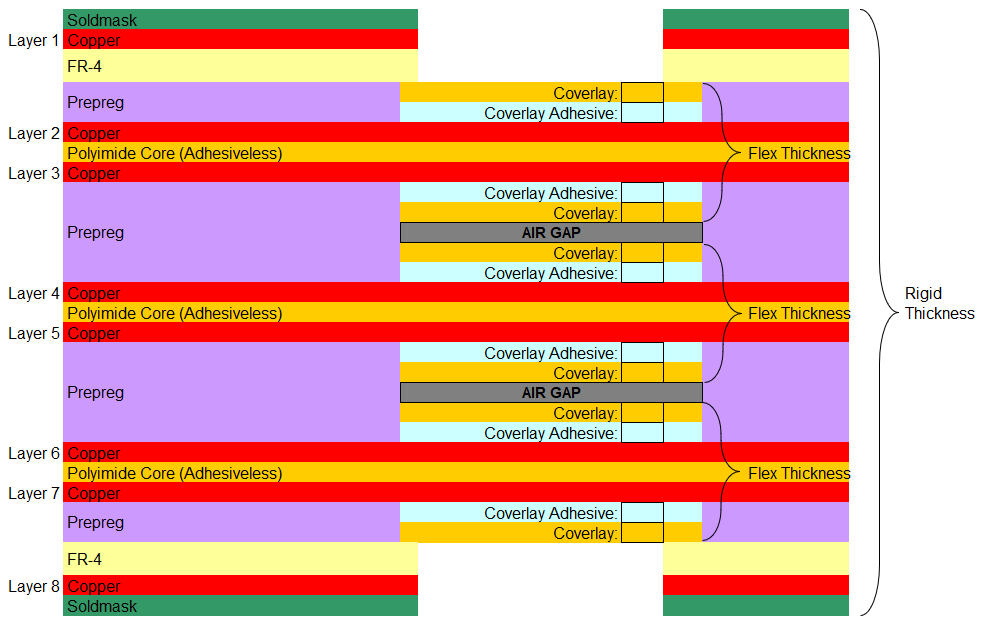
Example of an 8-layer rigid-flex PCB stack-up with 6 air-gap flex layers.
Via Reliability
An air-gap construction completely addresses the via reliability concern and results in a via structure as reliable as that of a rigid only printed circuit. With the flex layers configured as independent pairs, or sets, the flex layers are separated only by FR4 based pre-preg within the rigid areas. This results in both a higher bond strength, between layers, and eliminates all flexible adhesives from within the rigid areas and with it the high co-efficient of expansion issue.
The reliability of an air-gap construction has been proven through testing using IPC’s Interconnect Stress Test method. This test rapidly temperature cycles a sample of a specific construction. An air-gap construction exceeds the number of cycles for a pass result while a rigid-flex with 4 flex layers laminated together will fail.
An air-gap construction does require additional process steps as each flex pair requires coverlay on both sides, but this is easily outweighed by the saving from improved reliability and after assembly yields.
Mechanical Flexibility & Bend Reliability
Mechanically, the bend capability and reliability are significantly improved by an air-gap construction. The improvement is due to a combination of two elements. The first is that for each individual flex pair the flex thickness is significant reduced as compared to that of a completely laminated structure. This reduces what is referred to as the “I-Beam” effect. The second is that each flex pair is allowed to bend on its own based on its specific thickness without significant interference from the rest of the flex pairs. That is within reason. When bent, the individual flex pairs are allowed to take their own natural radius but at a point the flex pairs may come in contact with one another as the air-gap spacing between pairs is consumed. Under a severe “U”-shaped bend requirement and due to the slight difference in bend radius between pairs, the flex pair on the outside of the bend may constrain the inside flex pair to the point where it may start to buckle. This situation must be avoided as any buckling of a flex pair will exceed the material capabilities resulting in cracked circuits.
If the bend requirement is that of an “S” shape this issue does not occur as the 2 bends comprising the S shape cancel out the differences in bend radius between pairs.
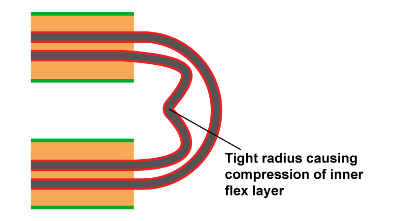
Example of severe u-shaped bend with buckled inside flex pair.
Summary
An air-gap construction is the preferred solution to higher layer count rigid-flex PCB designs. It provides the ability to reliably achieve tighter bend requirement and eliminate any via plating reliability concerns. Bend the few specific examples in the blog there are wide variety of air-gap configurations available that address many different design challenges.
Please feel free to contact Epec to discuss your specific design needs and to have your construction requirements reviewed to ensure the reliability of your design.
Key Takeaways
- Air-gap construction improves mechanical bend reliability by reducing overall flex thickness and minimizing the “I-beam” effect, allowing individual flex pairs to bend independently without overstressing copper traces.
- Via reliability is significantly enhanced since the design removes flexible adhesives from rigid areas, eliminating thermal expansion mismatches that can cause cracks in via plating.
- IPC standards allow 2-3 flex layers per set, with two layers being the most common for high-reliability applications. This segmentation maintains performance without over-thickening the flex areas.
- Air-gap designs pass IPC Interconnect Stress Tests more consistently than laminated 4+ layer flex structures, proving superior long-term reliability in temperature-cycling environments.
- The method requires extra processing steps since each flex set needs coverlay, but the added effort is outweighed by higher yields, reduced field failures, and overall better performance in high-layer-count designs.
Watch Our Video:
Designing Flex and Rigid Flex PCB Stack-Ups with Advanced Software
See our in-depth tutorial on creating a stack-up using our advanced software! In this video, we walk you through the process of generating a new stack-up, starting with the default settings and customizing it to fit your specific requirements.


