


What is a void in the printed circuit board (PCB) world? A void is an un-plated area within the hole wall of the PCB drilled plated hole. Voids in hole barrels can be equally problematic in all types of PCBs. The number of layers contained within the PCB plays a part in the cost of the completed circuit board. The more layers within the card the more cost is added for manufacturing. However, a two-layer part can also be expensive to scrap.
In this blog post, we will discuss voids, processing, causes, and prevention.

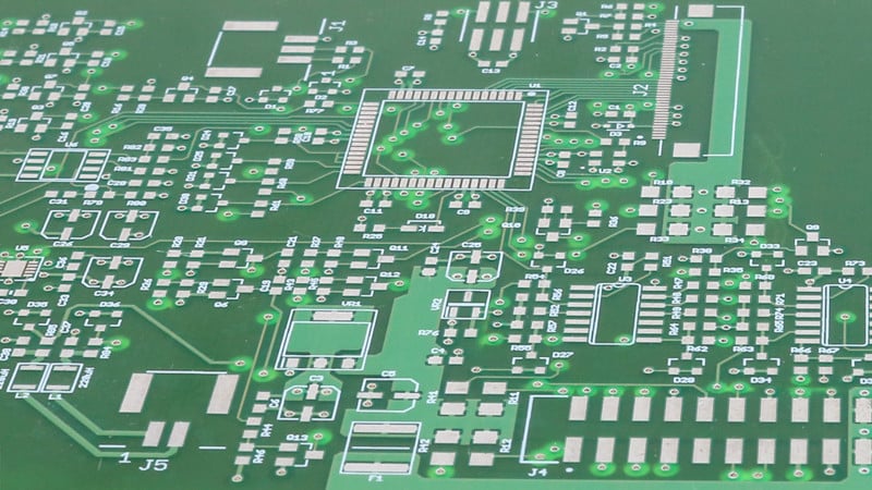
Printed Circuit Board Drilling Process
Whether you are building a 2-layer or multilayer PCB, the holes must be drilled either partially through or completely through the laminate material. The printed circuit board drilling machinery is computerized and programmed with the X, Y coordinates to drill each hole. The program is fed into the drilling computer, using selected tools to drill the individual sizes needed to complete the PCB drill process. Multiple circuit boards can be drilled simultaneously by several drill heads and by stacking more than one panel on top of the other. The drilling process is a time-consuming process that is costly. Each drill setting has a proper feed and speed for drilling the material, once the PCB is drilled, if it is not accurate it will be scrapped.
In the drilling process, the ultimate goal is to produce the part with a clean smooth barrel. When using the proper equipment and preparation the plating process will run smoothly. So, what can prevent the success of plating the perfect hole? A dull drill can inhibit the wall from being smooth as required for the plating process. The drilling process for a multilayer PCB will expose copper within the barrel of the hole for all internal electrical connections.
When the drilling process is completed, the surface of both sides of the master panel is deburred and the hole walls are cleaned, using a chemical solution to ensure proper hole cleaning, this is commonly known as desmearing. Debris is removed from the barrel and the internal connections that were exposed at the hole wall are prepped to allow properly connecting to the signals for the inner layers.
Multiple layer PCB with through vias connecting layers, either through thermal relief or direct to copper.
Annular Ring and PCB Design: What Should You Know About Drilling?
During the PCB layout process allowing for proper annular ring, the land around the hole allows continuity after plating. Without proper annular ring, the signal integrity can be compromised during the drilling process. During layout, the hole required for the components at assembly is a known value. It is a critical step to remember that all finished hole sizes are drilled oversized to allow for the plating processes. The typical oversize for plated holes is plus 0.005”, in other words, a finished desired diameter of .020” will be drilled at 0.025” size.
Internal layers do not have a plating process to add copper to the PCB surface and there are no through holes at this point in the process. The copper weight required by the designer is the copper that is used for the inner layer during the manufacturing of the PCB. Etching or removal of unwanted area copper will decrease the circuity and the annular ring. Allowing for the etch compensation of all copper allows for better electrical current passage.
What is a Plating Void?
A plating void is an area within the hole barrel of the PCB that is not plated properly during electroplating. One reason a void happens is due to the improper preparation of the hole wall. Dull drill bits will leave the wall of the hole rough and difficult to plate. Debris in the hole can also become dislodged, taking the plating away from the hole can also leave a void. This can be caused by not cleaning the holes after the drill process. Particles or contaminates in the hole prevent the plating chemistries from adhering properly. When the copper cannot properly adhere to the wall causing a skipped area or a void when the debris breaks away from the hole. Holes are inspected, plating is measured on the hole wall however it is difficult to inspect every hole for debris and impossible to check all for plating. AQL’s are performed and the process is closely monitored.
There are some other items worth mentioning that can cause a void besides poor cleaning and poor wall quality. These are less common however a mentioning of these can ease some concern and calm the panic of voids. For example, poor racking of the PCB during the bath plating process, excessively small diameter holes that have bubbles within the barrel, and poor agitation in the bath to move the chemistries through the holes.
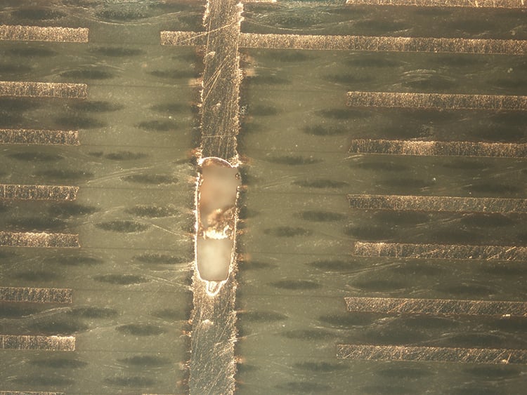
The microsection of plated through vias contains a void and is a multilayer PCB.
The plating within the holes conductively connects the areas of copper from the top side to the bottom and in some cases in between. When internal copper layers are exposed in the barrel wall the deposited copper creates an electrical connection to power the PCB. When there is a skip or a void in the barrel the current does not flow properly to the connections as needed for the proper functioning of the PCB. Signals fed through-hole walls are critical to the PCB to properly work after assembly. Once populated, the PCB is costly to scrap, component and raw cards can be hundreds to thousands of dollars.
How Do We Prevent Plating Voids?
The main suspect for plating voids is the drilling process leaving rough holes due to overused drills or debris left behind from drill bits. The individual drill bit does have a maximum number of times it should pierce the laminate and should be resharpened or discarded. Drills are expensive, most manufacturers prefer to resharpen and reuse the bit. Production should maintain strict records of hit counts, feeds and speeds, and the number of times the bit is sharpened to properly discard the old drill.
Along with proper cleaning of the hole wall and following processing procedures and work instructions is the best practice for avoiding the issue of voids. Maintaining proper racking, monitoring agitation within the tanks. Chemical analysis and plating process thickness monitoring are essential to be sure everything is being done to meet specifications.
Summary
As consumer demand for smaller and more powerful items for their everyday use, the components used on printed circuit boards have risen. The cost of circuit boards for process has also increased. A fully populated PCB scrapped for plating voids is extremely costly. Having your PCB supplier perform design for manufacturing review of the PCB layout can save costly issues during processing and assembly manufacturing.
Key Takeaways
- Voids are unplated areas that break electrical continuity: A plating void occurs when copper fails to properly coat the inner wall of a drilled hole. These defects can interrupt signal flow between layers, making the PCB unusable and often costly to scrap, especially after assembly.
- Drill condition and hole prep are leading causes of voids: Dull drill bits, improper feed/speed settings, and inadequate cleaning leave rough or contaminated hole walls that prevent proper plating adhesion. Strict control of drill usage and hole preparation is essential.
- Desmearing and cleaning are critical to successful plating: After drilling, holes must be chemically cleaned to remove smear and debris from inner layer copper. This allows the electroplating process to create a solid, conductive copper barrel wall.
- Smaller holes and poor tank agitation increase risk: Voids can also stem from small-diameter holes that trap air bubbles, improper PCB racking in plating baths, or insufficient chemical movement through the hole during plating. These less common causes still require close monitoring.
- Preventing voids requires a disciplined, data-driven process: Manufacturers must track drill hit counts, monitor chemical bath parameters, ensure thorough agitation, and follow IPC-recommended procedures. A robust DFM review by your PCB supplier can catch design issues that might increase void risk.


