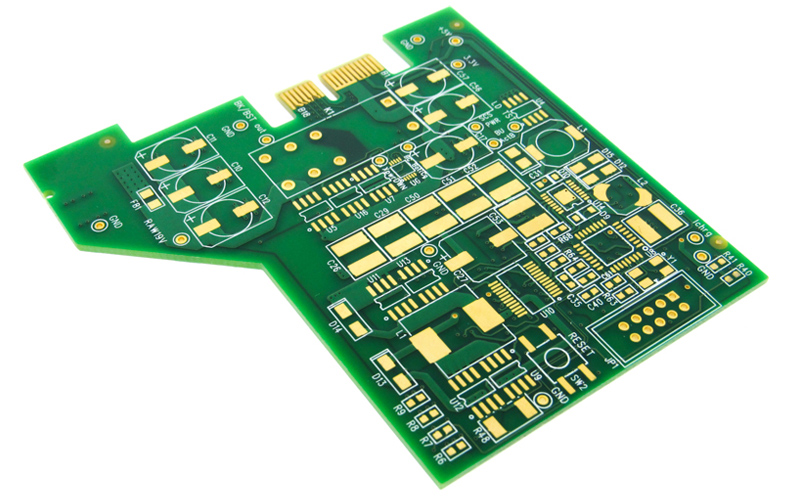
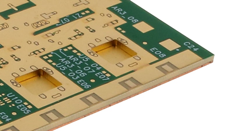
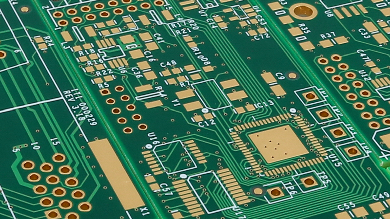
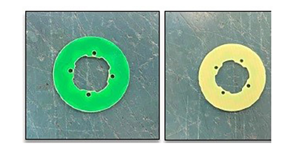
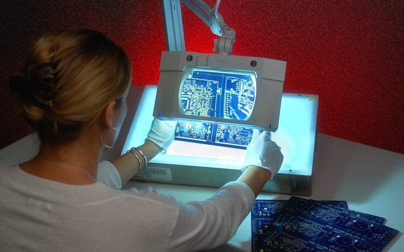
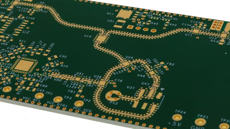
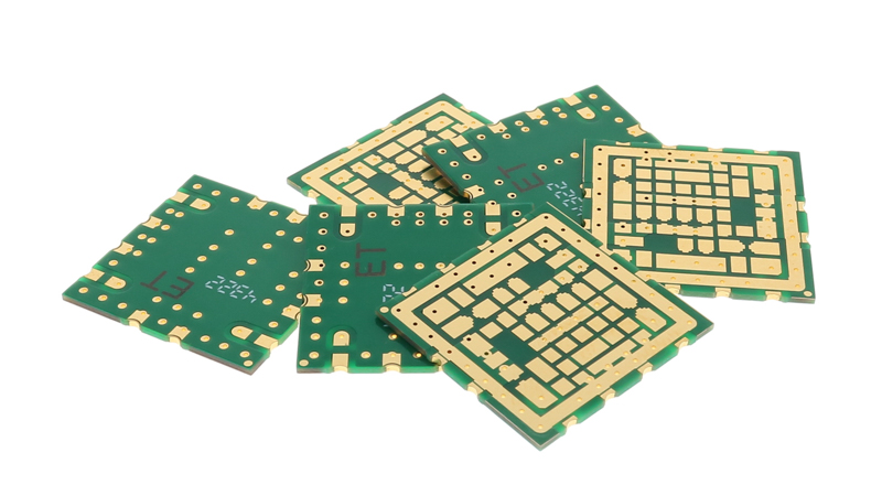
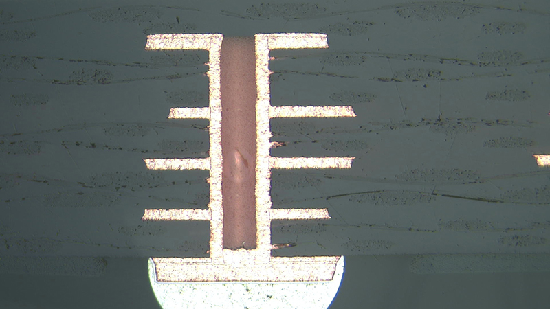
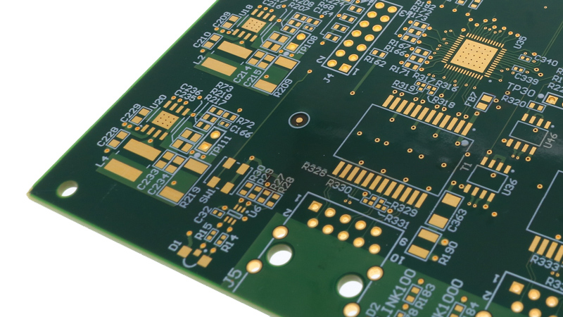
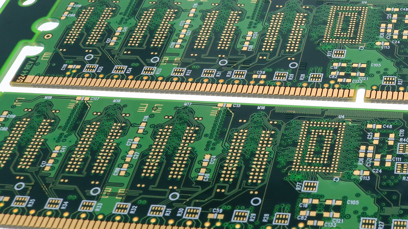
Navigating the world of printed circuit boards (PCBs) can be complex, especially when it comes to pricing. Unlike off-the-shelf products, PCBs are custom-engineered, each having unique specifications and functionalities. Understanding how these specifications contribute to the overall cost is crucial for effective planning and decision-making.
Read MoreDeveloping a successful RF printed circuit board (PCB) design requires careful consideration of various factors to ensure optimal performance and reliability. RF PCBs are essential components in wireless communication systems, radar systems, and other applications that rely on radio frequency signals.
Read MoreAt the conclusion of our webinar, Low Layer Count PCBs – Why They Are Not All Created Equal, we had several questions submitted to our presenter, Ed McMahon, CEO at Epec. We have compiled these questions into a readable format on our blog.
Read MoreIn the realm of printed circuit board (PCB) engineering, the design incorporates through holes as a means to establish connections across the board's various layers or secure the card during the assembly process. These through holes come in two distinct categories: plated and non-plated.
Read MoreFrom powering everyday gadgets like smartphones and laptops to complex systems in medical devices and aerospace technology, printed circuit boards (PCBs) are fundamental to modern electronics. They are essentially the heart and soul of all the electronic gadgets and devices that we use in our daily lives. For those in the PCB industry or even casual tech enthusiasts, understanding the basic principles of printed circuit boards is invaluable.
Read MorePrinted circuit board (PCB) laminates play a crucial role in the performance and reliability of electronic devices. Among the popular choices in the industry are Rogers and Taconic laminates.
Read MoreIn the world of printed circuit board (PCB) manufacturing, the devil is in the details. Even subtle design features like plated edges, castellated holes, and advanced milling techniques have far-reaching implications in terms of cost and production time.
Read MoreWrap plating is a technique used in the manufacturing of printed circuit boards (PCBs) to create a conductive layer that connects the layers of the PCB together. The process involves plating copper onto the walls of through-holes and vias in the PCB, which are then used to make electrical connections between the layers.
Read MoreAs I think about the processing of multi-layered printed circuit boards (PCBs), I find it interesting that in the early 1980s, I wouldn’t have dreamed of where we are today in terms of technology. I mean, think about it. Where we are in comparison to then is simply phenomenal.
Read MoreYou may be asking: what is an HDI printed circuit board and what makes it different than standard PCBs? Let’s break it down for better understanding from a design and from a supplier point of view. As Epec continues to grow our design business, it has become very apparent that many designers are very good at what they do and have no manufacturing knowledge to proof designs against.
Read More


