


While PCB layout typically has played the leading role in high-speed printed circuit board (PCB) applications, the role of the PCB fabricator becomes more and more important as the trend to faster, higher integrated, smaller form factors, and lower power electronic circuits become more prevalent.
The higher the switching frequencies are, the more radiation occurs on a PCB, which means that more process control is required from the circuit board fabricator in order to minimize the effect that this radiation can create.
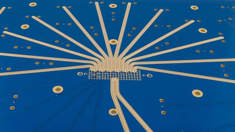
Example of a high-speed PCB design.
Manufacturing Considerations
How do you know when you should start looking at high-speed design and manufacturing considerations? Very simply: whenever the trace length becomes a significant fraction of a wavelength of the fastest signal, meaning that PCBs with large footprints need high-speed design solutions at lower frequencies than smaller PCBs since the trace lengths are longer.
This becomes a significant PCB fabrication issue in many instances because while the line widths may be larger on larger PCBs, and if a fabricator cannot hold a tight tolerance on a wider trace, then there can be wild swings in impedance.
For example, see the chart below:
| PCB Trace Width | Traditional Line width Tolerance | Value If the Line Width is Off By 5% |
|---|---|---|
| 50 mils | +/- 5% | 47.5 mils |
| 10 mils | +/- 5% | 9.5 mils |
Defining Impedance
Impedance is a combination of resistance and reactance in a circuit and controlling the impedance is critical when high-frequency signals are propagating on transmission traces on your circuit board. In this case, you will need to specify the impedance for a net or trace in order to preserve signal integrity.

In practice, if your traces are relatively short (takes more than 1⁄4 of the rise time of a signal for it to reach the end of the trace) or low frequency (under 200 MHz), then you may not need to worry about impedance control. High-frequency (RF) signals are typically run on controlled-impedance lines. That is, the trace maintains a characteristic impedance, such as 50 ohms (typical in RF applications).
How Does A PCB Fabricator Manage High-Speed PCBs?
Based on the formula for calculating the impedance of a trace, the following elements affect the characteristic impedance:
- Dielectric constant of insulating material – dK
- Thickness of insulating material
- Width of traces
- Thickness of traces
Starting with the most common material, FR4, it can generally be used in a high-speed digital design as long as the routes between components are not too long, which means smaller footprint designs. If you find that there is too much loss in your high-speed channel, you will need to consider selecting materials with different loss tangent characteristics.
There are numerous materials specialized for your high-speed signals such as PTFE-based laminates, spread glass laminates, or other specialized material systems available. This is the first place that the fabricator should be consulted for your designs for several reasons:
- Manufacturability of the Proposed Stack-Up – Many of the high-speed designs using hybrid designs (meaning more than one material type) are just not manufacturable. They have different properties that will not allow the finished PCB to be completed. Two very specific issues are how they react to heat when going through the press cycle and what happens to the laminate after it goes through etching.
- Availability of Materials – Many of the PTFE materials have very long lead times and very high minimum order quantities which will affect the delivery times, especially if it is a time-sensitive product. The other area that often gets overlooked is the availability of the thickness of the materials needed. It is critical for PCB designers to understand what the standard circuit board laminate thicknesses are in their fabricator’s stock so that they can adjust that variable only when it’s the last resort.
- Design Feature Consistency – Traditionally the tolerance for controlled impedance is +/- 10% which means that a fabricator needs to be able to control their process to maintain that specification. More and more we are seeing high technology customers looking for +/- 5% as a tolerance for impedance and while it is feasible, not everyone has the process control to manage this request.
Tips to Consider:
When you’re giving your PCB design to your fabricator, specify the impedance that you need not the dielectric thicknesses that you may have used to get to that impedance. This is for 2 reasons:
- Your fabricator can get to your impedance by adjusting the manufacturing recipe of dielectric thickness and line width which can dramatically improve lead time.
- If your impedance calculations are wrong, then that burden falls onto you as the fabricator built it to your specification.
Circuit Board Signal Integrity
Signal integrity starts with designing to a specific impedance value in your board and maintaining that during layout and routing. As PCB fabricators, we are only as good as the design that we provide. Some PCB design strategies to ensure signal integrity include:
- Aim for shorter routes between components to ensure high-speed signals.
- Try to minimize routing through vias, ideally only using two vias into and out of an internal layer.
- Layer stack-up should be constructed to have ground planes in layers adjacent to impedance-controlled signals so that consistent impedance is maintained.
- Eliminate stubs on ultra-high-speed lines with back drilling. Make sure that your fabricator has this capability.
- Pay attention to the need for any termination resistors to prevent signal reflection.
- Consult with your fabricator on which materials and processes can help you avoid fiber weave effects.
- Minimized length mismatches to prevent skewing and enforced spacing between traces to ensure differential impedance targets are met.
- Use a rough crosstalk calculation or simulation to determine the appropriate spacing between nets in your circuit board layout.
Check out some additional websites and resources that should be used as resources for PCD designers who are working on high-speed applications.
Summary
Your PCB fabricator should be brought into the fold early in your design process. We have discussed above all of the technical merits of using an experienced PCB fabricator like Epec. We haven’t even discussed the cost issues associated with these types of designs. Too often technical requirements and cost targets do not match which is how your PCB fabricator can help you compromise and get close in both aspects.
Key Takeaways
- Impedance control is critical: High-speed designs require precise impedance management, influenced by dielectric material, trace width and thickness, and insulating layer properties. Even small deviations can disrupt signal integrity.
- Material selection impacts performance and manufacturability: Standard FR-4 can work for shorter, lower-loss routes, but higher frequencies often demand PTFE or other low-loss laminates. Designers must also consider lead times, cost, and stock thickness availability.
- Fabricator involvement is essential: Hybrid builds and tight tolerances (+/- 5%) can introduce challenges that only experienced PCB fabricators with strong process control can handle effectively.
- Design strategy drives signal integrity: Shorter trace routes, minimized vias, adjacent ground planes, differential pair spacing, and techniques like back drilling all help maintain consistent high-speed performance.
- Specify impedance, not dielectric thickness: Providing the impedance requirement allows the fabricator to fine-tune the stack-up for accuracy and faster lead times, while also reducing the risk of design errors falling back on the customer.


