


Lowering PCB cost is primarily driven by design decisions made before layout begins, including layer count, board thickness, drill strategy, surface finish, and material selection. Small changes to copper layers, via structures, and panel utilization can significantly impact manufacturability, yield, and overall pricing.
Early collaboration with a PCB manufacturer helps avoid costly features and improves both performance and cost outcomes.

Cost Control Starts Before PCB Design
Cost reduction is most effective before Gerber files are finalized. Once a design is complete, opportunities to reduce cost without redesign are limited.
Close collaboration with your PCB manufacturer during the pre-design phase allows for:
- Optimization of layer count and stack-up
- Avoidance of expensive processes such as via-in-pad
- Selection of standard materials, finishes, and drill strategies
- Improved manufacturability and yield
Cost considerations extend beyond the bare board. Components, procurement volumes, and assembly processes all contribute to total cost, so design flexibility at the beginning of the project provides more opportunities to reduce overall spending.
PCB Layer Count and Overall Thickness
Layer count is one of the primary cost drivers in PCB fabrication. Each additional copper layer increases processing complexity and cost.
- The total number of copper layers (excluding solder mask and legend) directly impacts pricing
- Reducing layer count lowers cost, but must not compromise electrical performance or routing requirements
- In some cases, adding layers can improve trace and space capability, which can reduce manufacturing complexity
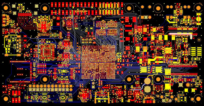
Example of a Multi-layer PCB Design with ground layers omitted.
Trace and space considerations are critical. Designs that push below 0.005” trace/space create additional manufacturing difficulty. Adding layers to allow for more relaxed trace/space can improve yield and reduce cost.
Thickness and Aspect Ratio
Overall PCB thickness is measured from top to bottom of the finished board.
- Thicknesses greater than 0.062” are typically treated as special builds with added cost
- Thickness impacts aspect ratio, which is calculated as:
Aspect Ratio = PCB Thickness ÷ Smallest Hole Diameter
Higher aspect ratios make plating plated through-holes more difficult, increasing risk and cost. Increasing hole diameter or adjusting thickness improves manufacturability.
Drill Count, Sizes, and Via Strategy
Drilling is a significant contributor to PCB fabrication cost.
Best practices:
- Minimize the number of unique drill sizes
- Use common hole sizes that support multiple components
- Increase hole diameters where possible to improve plating reliability
- Combine drill requirements across the design
Via considerations:
- Avoid via-in-pad unless absolutely required, as it adds significant processing complexity and cost
- Limit the use of blind and buried vias
- If blind/buried vias are required, minimize multiple sequential lamination cycles and keep them to one side when possible
Reducing drill complexity improves throughput and reduces machine time.
PCB Size, Shape, and Panel Utilization
Circuit board size and geometry directly influence manufacturing efficiency and cost.
Panelization considerations:
- Typical master panel size is approximately 22 x 16 inches
- Smaller circuit boards allow more parts per panel, reducing cost per unit
- Efficient panel usage improves yield and throughput
Shape and routing:
- Rectangular and square shapes maximize panel utilization
- Irregular shapes or angled edges require routing instead of scoring
- Routing increases processing time and cost compared to scoring
For example, small dimensional changes can reduce how many boards fit on a panel, doubling cost in some cases.
Surface Finish Selection
Surface finish affects both cost and manufacturability. Below are some of the common finishes.
ENIG (Electroless Nickel Immersion Gold)
- Most commonly requested finish
- Higher cost, but widely supported and reliable
- Typically processed in-house by manufacturers
OSP, Immersion Tin, LF-HASL
- Often require outsourcing to third-party processors
- Can introduce additional cost and lead time
HASL
- Legacy process containing lead
- Not RoHS compliant
- Less suitable for fine-pitch surface-mount designs due to uneven surface
Selecting a finish that aligns with both performance requirements and supply chain availability helps manage cost.
Materials, Tg, and Copper Weight
Material selection impacts both performance and cost.
Tg (Glass Transition Temperature)
- FR4 135Tg is common but less suitable for multiple solder cycles
- 170Tg materials are widely available and provide a good balance of cost and performance
- 180Tg materials offer higher thermal resistance but are less commonly stocked and more expensive
Specifying Tg or IPC-4101 slash numbers is preferred over calling out a specific brand, as it provides sourcing flexibility.
Copper Weight
- Standard weights: ½ oz and 1 oz copper are most commonly stocked
- Heavier copper (2 oz and above) increases cost and may have limited availability
Balanced copper distribution across layers improves manufacturability and reduces risk during fabrication.
Key Cost Drivers and Tradeoffs
The following design decisions have the greatest impact on PCB cost:
- Layer count and stack-up complexity
- Trace and space requirements
- PCB thickness and aspect ratio
- Drill count and number of unique hole sizes
- Use of advanced via structures
- Surface finish selection and processing availability
- Material type and Tg rating
- Copper weight and distribution
- Panel utilization and board geometry
Balancing these variables early in the design process leads to more cost-effective outcomes.
Summary
Design-driven decisions made before layout have the greatest impact on total PCB cost. Factors such as layer count, overall thickness, aspect ratio, drill strategy, surface finish, and material selection all directly influence manufacturability, yield, and pricing.
By prioritizing standard materials, simplifying via and drill requirements, and optimizing panel utilization, teams can reduce fabrication complexity and avoid unnecessary costs while still meeting performance requirements.
Key Takeaways
- Engage with your PCB manufacturer before design begins to identify cost-saving opportunities.
- Keep layer count and thickness within manufacturable ranges while meeting performance goals.
- Simplify drill requirements and avoid complex via structures where possible.
- Select widely available materials and finishes to reduce cost and supply risk.
- Design board size and shape to maximize panel efficiency.


