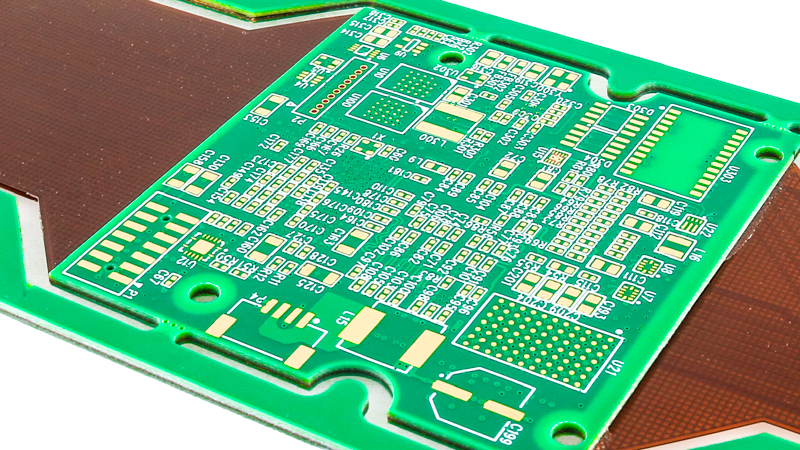
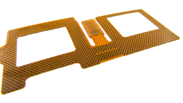
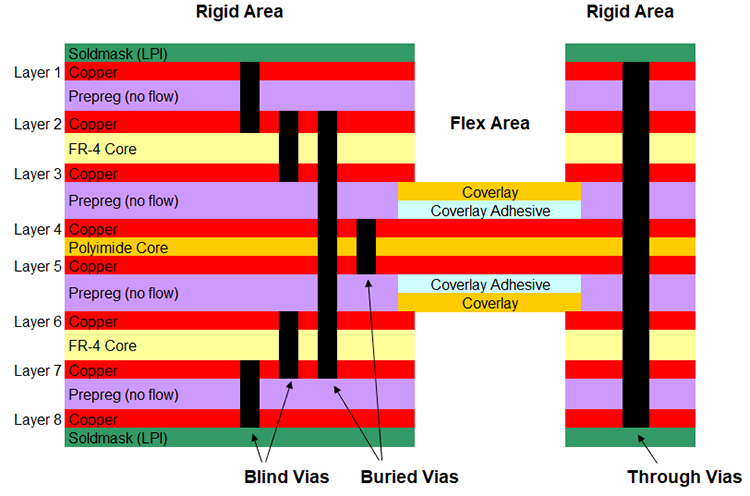
Heat dissipation is the ability of a part, whether a circuit or any other component, to take the heat that's being generated by a component or an element of the design and to distribute it, dissipate it, and make the heat go away, for lack of a better phrase. This prevents the temperature of the part from continuing to elevate as the device is operated.
Read MoreFlexibility is a critical element in most flexible circuit board designs. Whether it’s to meet a tight “one-time bend-to-fit” application or a “dynamic” infinite bend cycle application. To meet these requirements, a flex circuit design must be kept as thin as practically possible, use the correct copper type, and utilize the correct copper plating process.
Read MoreMechanical bend reliability is a critical element in a successful flex or rigid-flex PCB design. One area that can have a significant impact is the transition line(s) that occurs from a rigid area, in a rigid-flex circuit design, or from a stiffened area, in a flex circuit with stiffeners design, to the flex layer(s) only areas.
Read MoreDome switches are a very popular solution for use as a momentary switch. They are a good solution that provides tactile feedback that the switch has been depressed and an event registered. Many applications require a dome switch mounted to a flexible circuit board.
Read MoreWe get many inquiries from our customer base regarding updating or converting an existing design from its current configuration of rigid printed circuit boards interconnected with a wiring harness to a rigid-flex printed circuit board. With our experience, we can quickly determine if a conversion option is worth investigating further. We can also see how some are relatively obvious that they would need a complete redesign to convert.
Read MoreDating back to 1952, we are industry leaders and experts in all things printed circuit board (PCB) related, rigid PCBs, flexible circuits, and rigid-flex circuit boards combined, we know all the options and the difficulties in the fabrication processes. In this blog, we will focus on flex and rigid-flex PCBs what you should know and what to look for regarding the design and layout, as well as the importance of a successful data set and what is needed to prevent delays in engineering and manufacturing.
Read MoreAt the conclusion of our webinar, EMI Shielding Methods for Flex & Rigid-Flex PCB Designs, we had several questions submitted to our presenter, Paul Tome, Product Manager of Flex & Rigid-Flex Circuits at Epec. We have compiled these questions into a readable format on our blog.
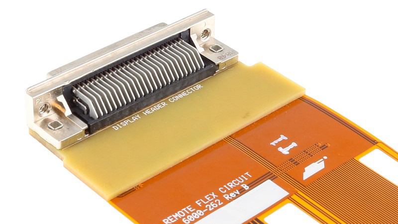
Read MoreFlex circuits have the capability of utilizing a wide variety of connector options. The list, with a couple of exceptions, includes all connector systems that can be used on rigid printed circuit boards (PCBs) plus a couple of additional systems that were specifically designed for interconnecting flexible circuits to rigid PCBs or wiring harnesses.
Read MoreThe last 18 months have been some of the most challenging that many of us have had to deal with both personally and professionally. It has often felt like we were riding waves, coming closer to things getting a little more normal, only to have them change radically. Looking forward to the next 18 months, I don’t see those changes getting any easier for us or our industry.
Read MoreWith advancements in rigid-flex PCB design technology, the use of laser-based systems in the manufacturing process are very common in the industry. Not having laser drilling and cutting available would place significant limitations on what could be accomplished in a design and what components could be used.
Read More


