


Higher current carrying flex circuit designs create challenges that need to be addressed early in the design process to ensure both a manufacturable design and that it will reliably meet the bend requirements. These items range from material types/availability, bend capability/flexibility, impact on standard signal lines, and part cost.
Copper is the stiffest component in a flexible PCB design and is also the critical element to the functionality of the circuit. In general, the standard flex design practice is to use the thinnest copper possible to achieve the highest degree of flexibility and bend reliability. The thicker copper needed to support the current levels and its compound impact on materials and construction will considerably reduce the bend capabilities of a given design. This needs to be reviewed and, in many cases, tested to ensure a reliable design.

In this blog, we will cover a range of design and material elements that are impacted by the higher current levels and design strategies that will help lessen the impact of the thicker copper requirements.
Material Availability
The flexibility requirements of many flex circuits limit the standard available copper thicknesses from material suppliers to 2 OZ or thinner. If a design requires more than 2 OZ copper, to safely handle the current levels, there are three options to consider: special order materials with thicker copper, increase copper thickness with additional surface plating, or manufacture core material in house.
The first option of special-order materials, if available, is costly and time-consuming, but has the advantage of using an adhesiveless construction, which reduces the overall flex thickness.
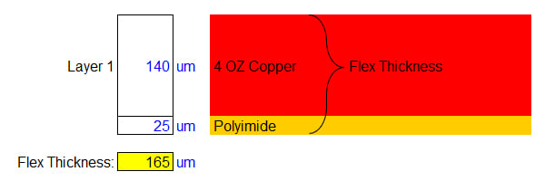
Example of a flex circuit copper thickness.
The second option of added surface plating is a practical solution that allows for up to 3 OZ finished copper thickness consisting of a 2 OZ base copper + 1 OZ of added plated copper. A negative element is that while the base copper can be of the preferred rolled annealed format the added plating will be electro-deposited copper, which has a lower degree of bend capability.
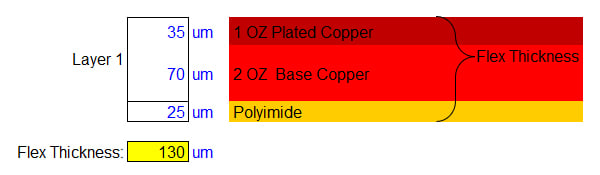
Example of a flex circuit with added surface plating.
The third option of making the material may be a practical solution. It requires purchasing the required copper thickness separately in sheet form and then laminating it to a layer of polyimide using a layer of flexible adhesive. The advantage is the design will consist only of rolled annealed copper without any additional surface plating. The negative aspect is that the core thickness will increase due to the added adhesive layer(s). An adhesive layer is required for each copper layer in the design.
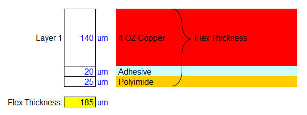
Example of a flex circuit with adhesive layer.
Coverlay Requirements
Copper thickness also impacts other materials in the flex construction. Coverlays are attached by means of a flexible adhesive. It serves to both attach the coverlay to the circuit and to encapsulate the spaces between adjacent traces. A standard guideline is a minimum of 0.001” of adhesive is needed for each 1 OZ of copper thickness. This ensures enough available adhesive to ensure a proper void-free lamination and adds significant thickness to the design, which further limits the bend capabilities. However, the starting coverlay adhesive thickness is not what will be present in the finished circuit. During the lamination process, the adhesive thickness is reduced as it flows to encapsulate the underlying circuit pattern. The percentage reduction will be dependent upon the ratio of line widths to spacing in a given area. Circuits with large spacings will see a greater thickness reduction than higher density designs or designs with wide traces and or copper fill areas.
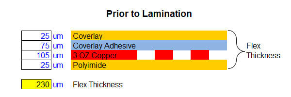
Example of a Coverlay prior to lamination.
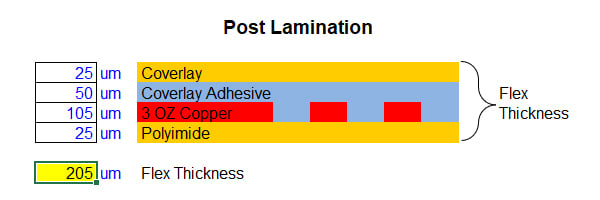
Example of a Coverlay post lamination.
Combination High Current + Low Level Signal Designs
Designs that combine both high current carrying with standard level signals adds additional design elements. The minimum line width available for use in the signal lines will be based on the base copper thickness used. For example: 2 OZ base copper requires a 0.007” minimum line width and spacing. This increases as the copper thickness increases.
Designs that also have controlled impedance further increase the flex thickness and reduce the bend capabilities. Thicker cores are necessary to achieve the specific impedance values. The core thicknesses is then further increased by the wider than typical line widths driven by the copper thickness.
Design Strategies to Reduce Thickness and Improve Flexibility
There are several design strategies that help mitigate the negative impact on flexibility that comes with higher current carrying requirements.
A primary strategy is to maximize the flex area width. This then may allow for the use of wider circuits with thinner copper to safely carry the current. This has the positive impact of reduced flex thickness, reduced coverlay adhesive thickness, improved flexibility, material availability, and reduced cost. Two-layer designs may have available space on the secondary layer to allow high current lines to be split and run parallel on both layers again with thinner copper.
If a design requires both higher current and controlled impedance, consider separating the two needs into independent flex layer pairs within a rigid-flex with air gap construction. This allows each flex layer pair to utilize the materials and construction required to meet its specific requirements rather than having them compound each other.
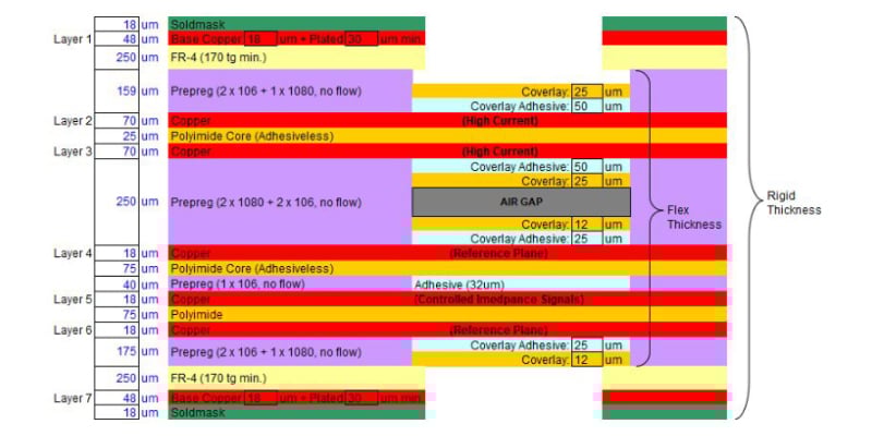
Example of a rigid-flex PCB stack-up that mitigates the negative impact on flexibility.
In a worst-case situation, it may be needed to divorce high current signals from the standard signals in to two separate circuits. This may consist of two either independent flex circuits or a combination of a flex circuit and a wired solution to carry the current lines. This allows the needs of the specific independent circuits to be achieved without the negative impact of them compounding into a construction that cannot be manufactured or will not meet the mechanical bend requirements.

Summary
Higher than standard current levels create design challenges that must be reviewed fully to ensure that the mechanical bend requirements are met, and the finished part is reliable. As with many flex aspects of flex design, there are material and designs options that can allow the design objectives to be achieved. Please feel free to contact Epec if you have any questions regarding the design of your high-current circuit application.
Key Takeaways
- Copper thickness limits flexibility: The thicker copper required for high-current designs significantly reduces bend capability. Standard flex practices favor the thinnest copper possible, so higher current designs must be carefully tested to ensure mechanical reliability.
- Material availability is a constraint: Flex materials are generally limited to 2 oz copper. Exceeding this requires special-order materials, additional plating, or in-house lamination, each with trade-offs in flexibility, cost, and manufacturability.
- Coverlay adhesive thickness increases with copper: A minimum of 0.001" adhesive is needed per 1 oz of copper to ensure proper lamination, which adds thickness and further reduces bend performance. Line width-to-spacing ratios also influence final coverlay thickness during lamination.
- Mixed high-current and signal circuits create added complexity: Higher copper thickness drives up minimum line widths and spacing, impacting standard signals and controlled impedance designs. This often requires thicker cores, reducing bend reliability.
- Design strategies can reduce impact: Options include widening the flex area to allow thinner copper, splitting current paths across multiple layers, separating high-current and controlled impedance sections into rigid-flex structures, or, in extreme cases, separating circuits entirely to maintain manufacturability and performance.


