


In some areas of a flexible circuit board design, the trace widths and spacings, trace to pad spacings, and via pad sizes are the same as used in rigid circuit boards but will differ in other areas. This is due to the flexible nature of the polyimide materials used, the type of material used to encapsulate the external layers, and the unique plating process used for most flex circuit designs.
All of these elements, either singularly or combined, require that sizes and spacings be increased from the typical minimums used in a rigid PCB design. Flex materials have larger dimensional tolerances than rigid circuit board materials as they are flexible and do not have glass re-enforcement. These tolerances come into play when the circuit patterns are etched and when the materials are subjected to heat, pressure, and moisture during the manufacturing process.
In this blog, we will review the specifics of trace widths, spacings, via, and via pad sizing as they apply to a flexible circuit design.

Trace Widths and Spacings for Flexible PCB Designs
Trace widths and spacings in a flexible PCB design, in all areas other than traces adjacent to SMT + PTH pads, are essentially the same as those used in rigid PCB designs. The control factor is the thickness of the base copper being specified.
The standard industry rules for are as follows:
- 1/3 OZ copper: 0.003” trace and space
- 1/2 OZ copper: 0.004” trace and space
- 1 OZ copper: 0.005” trace and space
- 2 OZ copper: 0.007” trace and space
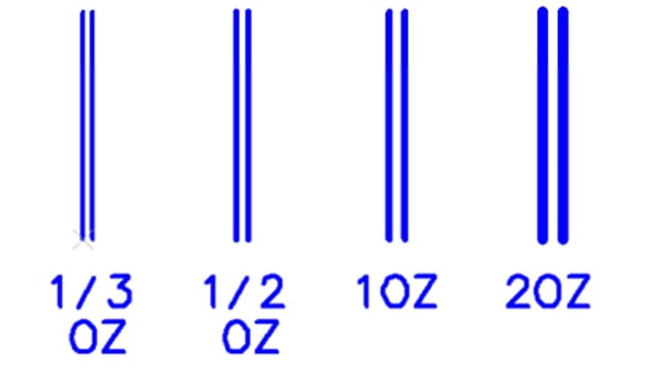
Copper thicknesses greater than 2 OZ are seldomly used in flex circuit designs as they have a significant negative impact on flexibility and bend capability.
The type of copper also differs from rigid circuit boards. Most flex circuit designs use copper that starts as the electro-deposited copper, used in rigid PCBs, but is then processed to become rolled annealed. This converts the copper grain structure from a vertical orientation to an elongated horizontal configuration, which provides a higher degree of ductility.
It is also very common in flex circuit designs that no additional copper is plated onto the surface of the traces when plating the holes. The base copper is the finished copper thickness to provide greater flexibility and maintain the added bend reliability that the rolled annealed base copper provides. We will cover this plating process in more detail later in this blog.
Trace Spacing to Pads Requirements
One area where spacings can vary in flexible circuit board designs is where a trace passes adjacent to a pad. If the pad is used for a via hole, then the spacings remain the same as previously defined for the various copper thicknesses. However, if the trace is adjacent to an external SMT or PTH pad then additional flex material dimensional tolerances and the type of material used to encapsulate the circuitry need to be factored in.
For polyimide coverlay, the trace-to-pad spacing must be increased to a typical min. of 0.010” to prevent an exposed trace or coverlay on the pad. The coverlay has the same material tolerance as the flex core. It also has the added element that all the SMT & PTH openings are mechanically created prior to it being positioned and laminated to the flex circuit surface. These added openings can dimensionally destabilize the coverlay, adding additional tolerances and in turn additional spacing requirements.
If a flexible soldermask is being used, then the additional spacing required is less than that of coverlay, approx. 0.006”, as then is no additional material tolerances. It is applied in the same manner as on rigid PCBs.
To address the above challenge, it is common in many designs to use a hybrid configuration of both coverlay and soldermask on the same layer. The soldermask is used locally in tight spaced component areas, and coverlay is used in the balance of the part.

Example of trace to adjacent pad spacing.
Via Hole and Pad Size Requirements
Via and via pad sizing are impacted by both the material dimensional tolerances and by the plating process that differs from that used on rigid PCBs. The plating process, known as either “selective pad plating” or “button plating” and why it is used will be described in more detail further on in this blog. Undersized via pads is one of the most frequent design issues we encounter.
Via sizes can, in general, be much smaller than used in rigid PCBs due to the much thinner construction of a flex circuit. Thinner flex constructions reduce the aspect ratio (hole diameter vs. hole depth), which facilitates the plating process. A common drill size used is a drilled 0.008”. A drilled 0.006” and a lasered 0.004” via hole as also available.
The standard additional amount required for a via pad for mechanically drilled holes is a min. of + 0.010” (I.E: 0.008” with 0.018” pad). + 0.012 – 0.014” is preferred for improved yields in volume production and for larger designs where the dimensional tolerances accumulate to a greater degree. For a lasered 0.004” hole, the additional amount for the pad is reduced to 0.008”. This is due to the laser drill’s optical registration system being able to “zero” out some of the material tolerances.

Example of via pad size.
Selective Pad Plating Process
As previously mentioned, most flex circuits use a preferred selective pad plating (button plate) process. This method prevents any additional copper from being plated on the surface of the circuitry on the external layers. The plating is restricted to within the barrel of the plated holes and to a small ring of copper on the surface of the pad surrounding the hole. This is preferred as it maintains the copper at the starting base thickness and as only the preferred rolled annealed copper type. Both items improve the flexibility, mechanical bend reliability and the minimum bend radius capability of the design.
The selective pad plate is achieved by applying a photo imageable mask to the starting copper surface and then imaging and developing opening exposing all the plated hole locations. These openings are slightly larger than the hole diameters, to allow for material and process tolerances, resulting in the raised ring (button) of copper surrounding the hole itself. The height of the copper ring depends upon the layer count of the design and the IPC specified minimum copper thickness required. A 2-layer design requires a min. of 0.0005” copper plating thickness resulting in a 0.0007” – 0.0008” button height. A 3-layer or greater design requires a min. of 0.001” copper plating thickness leading to a 0.0012” – 0.0014” button height.
The selective pad plating process requires a via pad size due to the topography created by the button height. To image the circuit pattern and pads the photo imaging film must conform over the height of the buttons. A sufficiently sized flat land area, between the diameter of the plated button and the perimeter of the pad, is needed to maintain proper adhesion. This is part of the min. 0.010” pad to hole diameter oversize defined previously. Without this the photo imageable mask may flake off significantly reduce the manufacturing yield rate.
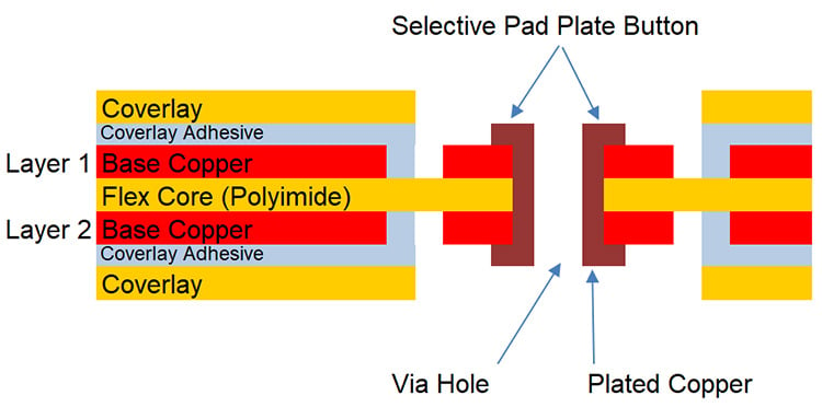
Cross section of a selective pad plated flex circuit.
Summary
Trace widths and spacing requirements for flex circuits differ from that used in rigid PCBs. This is necessary due to the different materials, the material properties/tolerances and the different manufacturing processes used. Please feel free to contact Epec to discuss your design requirements or to have your design reviewed for manufacturability.
Key Takeaways
- Trace Widths and Spacings Depend on Copper Weight: Flexible PCBs follow similar trace/space rules as rigid PCBs, with minimums ranging from 0.003" (for 1/3 oz copper) to 0.007" (for 2 oz copper). However, heavier copper reduces flexibility and is rarely used beyond 2 oz.
- Coverlay Requires Greater Trace-to-Pad Spacing: When using polyimide coverlay, trace-to-pad spacing must be increased to at least 0.010" to accommodate material tolerances and mechanical punching. Flexible soldermask allows for tighter spacing, around 0.006", and hybrid coverlay/soldermask approaches are often used.
- Via Pads Must Be Oversized to Ensure Yield: Flex circuits demand larger via pads than rigid boards to accommodate button plating and material stretch. A typical 0.008" via hole should have a pad at least 0.018", with +0.012" to +0.014" preferred for volume production.
- Selective Pad Plating Improves Flexibility: The button plating method limits plating to only via barrels and pads, keeping traces at base copper thickness. This enhances flexibility, improves bend reliability, and supports tighter bend radii.
- Laser-Drilled Microvias Allow for Smaller Pads: Laser-drilled vias (as small as 0.004") offer tighter tolerances due to optical alignment, requiring only 0.008" pad oversize. These are ideal for high-density or space-constrained flex designs.


