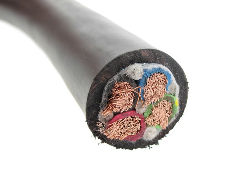
One of the most common reasons for selecting a custom cable assembly is to satisfy some type of flexibility or bending requirement. Even the bulkiest of electrical cables have some sort of give to them, allowing them to form around corners or be coiled.
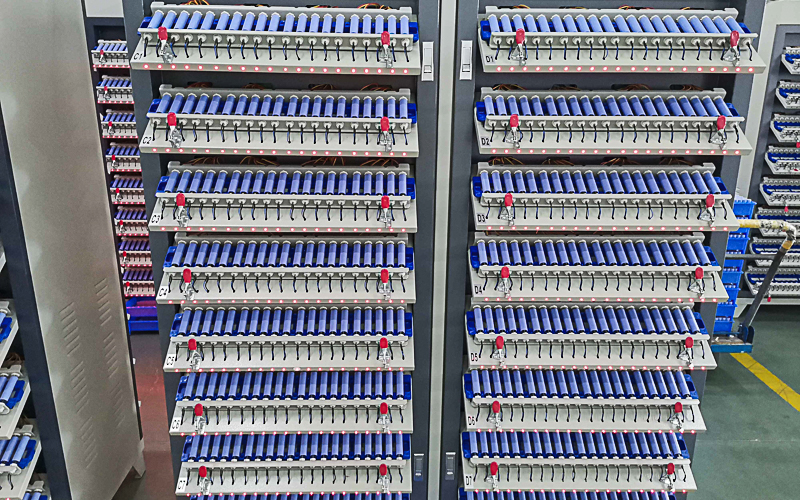
Read MoreCustomers who have products or applications using lithium-based batteries understand the risks involved in keeping the battery packs safe during manufacturing processes, when transporting them to specified locations and when they are in use.
Read MoreThere are many forms of Night Vision Imaging Systems (NVIS) that help our nation’s warfighters, pilots, and other professionals. Known as Night Vision Goggles (NVG), these devices are highly specialized and amplify various wavelengths of light allowing the user to “see” in darkness.
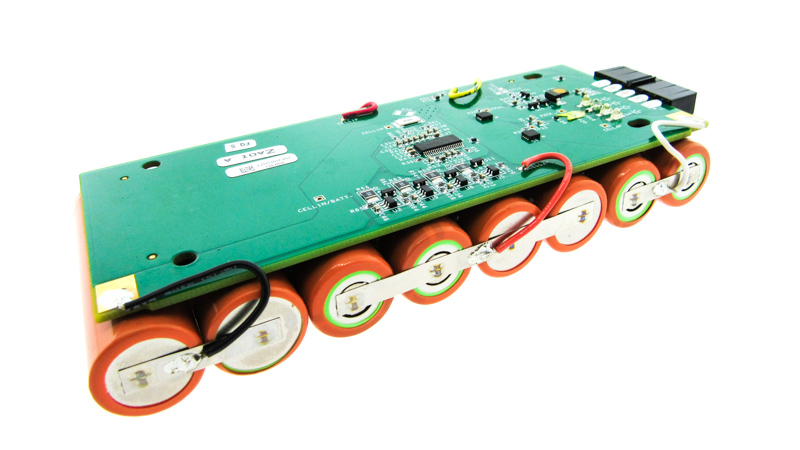
Read MoreSupplying custom battery packs to companies in aerospace, medical, military, oceanography, and other industries requires the skills and technical expertise provided by quality manufacturers such as Epec. Yet, the design and build of the battery pack is often only part of the customer's order.
Read MoreAs printed circuit boards (PCBs) progressed, requiring their functions to be more and more complex and diverse, the number of layers increased from 1-2 layers, up to 4-30 layers, with 4-12-layer boards being more typical.
Read MoreWith electronics becoming more portable and lightweight, they require batteries that offer long hours of battery life before recharging. Lithium batteries are becoming common place in electronics such as smartphones, laptops, and tablets as they can last for up to 2 years to 5 years. However, failures can cause lithium battery packs to malfunction. The type of problem will be based on the construction of the battery pack, how it is charged, how it is used and handled, and environmental factors.
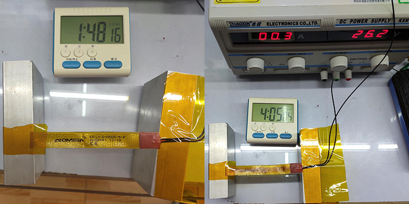
Read MorePolyimide flexible heaters are highly desired in industries such as aerospace, medical, food service, military, and others to provide controlled heat in specified areas in their applications. This heater type may be used in instrument panels inside aircraft to provide moisture-control properties and to prevent the systems from malfunctioning due to extremely cold temperatures at high altitudes. They may also be found in medical diagnostic devices, analytical test equipment, optoelectronic components, and many other applications.
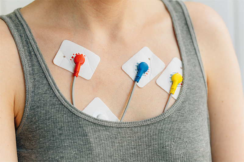
Read MoreCable assemblies used in the medical the industries have to be biocompatible, made of a material that will not cause issues or adverse effects when coming in contact with the body. The material should not cause any type of toxicity (whether it is to the skin or to internal organs, bone, blood, or tissues) that could endanger a person's health.
Read MoreOvermolded cable assemblies are widely known for their superior performance, attractive cosmetics, and the fact that they can be customized for nearly any application. But overmolded cables also require a sizable investment in hard tooling well before the first cables are ever produced.
Read MoreThose of us who make our livings managing supply chain, the time of the year between Halloween and New Year’s Eve is always on the tense side. Known as the “Peak Season”, it seems to start earlier and earlier the more people turn to e-commerce.
Read More


