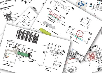




A great tool to catch printed circuit board (PCB) defects before they cause problems is the ability to identify process indicators. The earlier these process indicators can be identified in the PCB fabrication process, the greater the ability to avoid financial risk with the PCB builds. In high-reliability applications, waiting until final inspection to catch defects is too late. By that point, time, materials, and labor have already been invested, and the cost of rework or scrap can be high.
From a quality control perspective, PCB fabrication is not just about reacting to defects; it is about building systems that prevent them. This means understanding where problems are most likely to originate and putting controls in place at each stage of the process. The following areas represent some of the most critical checkpoints where early detection can make the biggest impact.
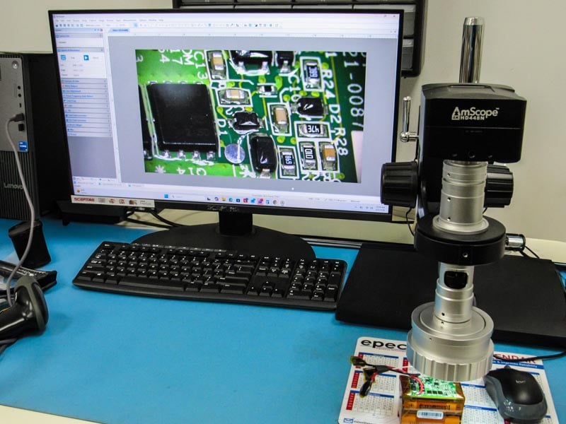
Final inspection using a 3D digital camera microscope.
Contract Review
Understanding all requirements in a customer purchase order is the best way to prevent defects. If something is missed here, the likely location of identifying the defect is after your customer has received fully fabricated parts, which is the worst-case scenario.
Purchase orders often contain more than just quantity and delivery requirements. Many customers include critical details that may not appear on fabrication drawings. These can include required build standards, certifications, testing requirements, or even specific material or marking instructions buried in the fine print.
A thorough contract review ensures that all expectations are aligned before production begins. This step is often underestimated, but it sets the foundation for the entire build. From a quality standpoint, it is far easier to clarify a requirement upfront than to resolve a discrepancy after parts have shipped.
Upfront Engineering Review
There are many times when Gerber data received from the customer may conflict with stated requirements, drawings, or industry standards. If these conflicts are not identified and resolved early, the result is almost always a defective product.

Common issues found during upfront engineering reviews include missing drilled holes, incorrect dimensions, spacing violations, trace width inconsistencies, and incomplete netlist data. These are not minor issues. Left unchecked, they can lead to electrical failures, assembly challenges, or complete product rejection.
A strong engineering review process acts as a gatekeeper. It ensures that the design is manufacturable, compliant with standards, and aligned with customer expectations. This step also provides an opportunity to communicate with the customer and resolve ambiguities before they become costly problems.
Drilling Process Control
The drilling process is one of the first physical fabrication steps, and it introduces several potential defect risks if not properly controlled. Proper cleaning and deburring of drilled holes is extremely important, as any residue left behind can impact subsequent processes.
If drilling debris is not removed, it can interfere with plating adhesion, affect surface finishes, and even alter the affected hole size. These issues may not be immediately visible but can lead to reliability failures later in the product lifecycle.
From a quality control standpoint, monitoring tool wear, maintaining clean drilling environments, and verifying hole integrity are key process indicators. Catching issues at this stage prevents defects from being carried forward into more complex and costly steps.
Desmear and Hole Preparation
Desmear, or hole preparation, is especially critical for multilayer PCBs. This process removes resin smear from drilled holes and prepares the surface for proper metallization. Poor control at this stage can lead to serious structural issues.
If desmear is not performed correctly, it can result in barrel cracks, poor adhesion of barrel walls, and eventual inner layer separation. These defects may not be detected until electrical testing or, worse, during field use.
Process indicators such as chemical concentration, exposure time, and surface cleanliness must be closely monitored. Consistency is key. Even small deviations can have a large impact on long-term reliability.
Plated Through-Hole (PTH) Deposition
The plated through-hole process is one of the most critical steps in PCB fabrication. This is where conductive copper is deposited within drilled holes to create electrical connections between layers.
If this process is not tightly controlled, defects such as copper voids, thin plating, or uneven deposition can occur. These defects compromise electrical continuity and can lead to intermittent failures or complete circuit loss.
Quality control at this stage involves monitoring deposition coverage, bath chemistry, and proper bath activation. Cross-section analysis and inspection are often used to verify that plating meets required specifications. Identifying process indicators early in this step prevents defective boards from progressing further down the line.
Building a Preventive Quality Mindset
Identifying indicators or defects at any of these early fabrication steps can be a tremendous cost and time saver by avoiding defects on fully fabricated parts. However, the real value comes from building a preventative quality mindset across the entire process.
Rather than relying solely on final inspection, successful PCB manufacturing operations focus on in-process controls. Each step is treated as an opportunity to catch and correct issues before they escalate. This approach not only improves yield but also strengthens customer confidence and reduces overall project risk.
In high-reliability industries such as aerospace, medical, and industrial electronics, this level of control is not optional. It is a requirement. The cost of failure in these applications far outweighs the cost of implementing robust quality systems.
Summary
Catching PCB defects early in the fabrication process is one of the most effective ways to reduce risk, control costs, and improve overall product reliability. From contract review to plating, each stage presents opportunities to identify process indicators that signal potential issues.
By focusing on early detection and maintaining strict process control, manufacturers can prevent defects from ever reaching the customer. In PCB fabrication, quality is not something that is inspected at the end; it is something that is built into every step along the way.
Key Takeaways
- Early identification of process indicators is the most effective way to prevent PCB defects and reduce overall project risk.
- Thorough contract review ensures all customer requirements are captured before production begins, avoiding costly misunderstandings.
- Upfront engineering reviews help identify design conflicts and manufacturability issues before fabrication starts.
- Critical fabrication steps such as drilling, desmear, and electroless plating require tight process control to prevent structural and electrical defects.
- A preventative quality approach, focused on in-process controls rather than final inspection, leads to higher reliability and better overall outcomes.