


There are a wide variety of flexible circuit board design options available to solve interconnect requirements. One of the more unique is a dual access flex PCB construction. This unique construction of a dual access flex circuit can be beneficial for many applications.
In this blog we’ll review the definition of a dual access flex circuit, the types of applications possible, how it is constructed, what design limitations exist, the data set requirements, and how to incorporate EMI shielding if required.

Dual Access Definition and Applications
A dual access flex circuit is a unique configuration that exists only in flex circuit design. To summarize: a dual access flex is a one-layer flex circuit that permits independent access to the one copper layer from both sides of the part. This allows component or contact placement capabilities of a 2-layer design but with only one circuit layer. PTH components/connectors are supported as well as ZIF contacts on both sides of the design.
This type of construction has the following advantages:
- Allows for a double-sided component design with very tight bend capabilities.
- Well suited to dynamic flex circuit applications. The copper layer is in the preferred center location, neutral bend axis, within a very thin construction.
- Potential cost-saving opportunities for some dual-sided applications.
The most common application is the flex circuit used to interconnect between ZIF connectors but this requires the ZIF contacts to be on opposite sides of the opposing ends of the part to meet the ZIF connector orientation requirements of the design. A straight pin-to-pin schematic is required, which is common for most ZIF-to-ZIF designs. As an extension, a dual access flex can be used for any type of straight-through design application with soldered connectors at each end. The connectors can be either PTH, SMT, or both, and again the requirement is that the connectors are facing the opposite sides of the design.
In addition, dual access flex circuits can also be applied to simple designs that require only one layer of circuitry routing combined with the element that some components must be assembled or inserted from one side and other components from the opposing side. A common scenario occurs when you have a combination of PTH and SMT components where the PTH devices must be installed from the opposite side of the SMT devices.
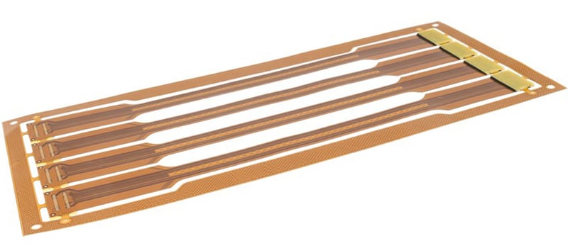
Dual access flex circuit with FR4 stiffeners.
Dual Access Flex Circuit Construction
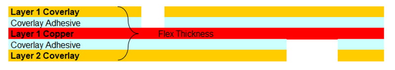
A dual access flex construction is manufactured by utilizing the properties/capabilities of the polyimide coverlay that is used to encapsulate the circuitry. Unlike the liquid-based soldermask used in rigid PCBs, coverlay is a solid sheet polyimide layer into which the required component pad openings are machined (i.e., laser cut or die cut).
The actual construction method is as follows. The circuit layer starts as a separate copper foil layer independent of a core material. A layer of coverlay, with its required component pad openings, is laminated to one side of the copper foil layer and then the circuit pattern is formed using the standard photo imaging and etching processes. A second layer of coverlay is then laminated to the opposite exposed copper side, with its necessary but different from the initial side component pad openings. The end result is a flex circuit with one copper layer laminated between two unique layers of polyimide coverlay with different openings in the coverlay from side to side creating the dual access capability.
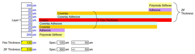
ZIF-to-ZIF dual access flex circuit.
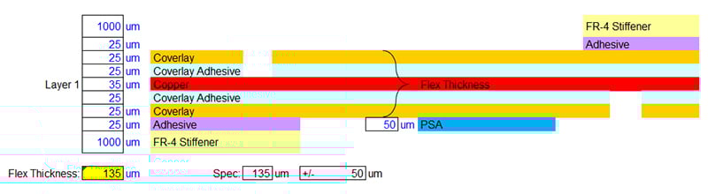
SMT to SMT dual access flex with FR4 stiffeners and PSA.
Design Capabilities and Limits
The design limits for a dual access flex circuit are like that of a 1-layer rigid board in that there will be only one layer of copper available for circuit routing. This limits the schematics to straight-through pin-to-pin, or very simple routings. As a 1-layer design, no circuits can cross one another. It may be possible to wrap circuits around the profile of the design to solve minor routing issues, but beyond that, there is no option of dropping in a via in and moving the circuit to a secondary layer so that it can cross under other circuits.
All available copper thicknesses can be utilized in a dual access flex PCB design. There is a general preference to 1 OZ copper, driven by ease of handling of the copper foil during manufacturing, but for higher density designs, 1/2 or 1/3 OZ copper can be used. The line widths and spacings capability for a dual-access design are the same as a rigid PCB or flex and will depend upon the copper thickness used for the design. For example – 1 OZ copper: Min. line width and spacing is 0.005”, 1/2 OZ copper is 0.004” etc. 2 OZ or greater copper thicknesses are also available for higher current carrying applications.
A unique capability in a dual access flex design is that copper features can also be exposed on both sides at the same location. This will however limit the copper thickness to 1 OZ or greater in most designs. With the copper feature(s) unsupported on both sides within the coverlay openings, thicker copper is necessary to provide sufficient strength to be mechanically reliable. A 2-sided exposed copper feature(s) must also dimensionally extend beyond the size of the coverlay openings so that the coverlays can retain the copper feature in place. Allowing the copper feature to suspend unsupported requires a minimum of 2-3 OZ copper to ensure it has enough strength. This however may impose design limits in the circuit density possible and the flexibility of the finished part.
Dual access flex circuits can use all the additional design elements found are standard 1 or multi-layer flex PCB designs. There are no limitations created by the dual access construction with respect to stiffener locations, stiffener materials, and PSAs.
Dual access flex with unsupported fingers and PSA.
Data Set Requirements
The data set for a dual access flex is straightforward. It's the same as a one-layer flex design with the exception that it includes 2 coverlay layer files instead of the usual 1-side file only. There will be a coverlay file for the topside with its unique opening’s configuration, and a second coverlay file for the bottom side with its unique opening’s configuration. The sizing of the coverlay openings follows standard design rules, however, for features exposed on both sides at the same location, the coverlay openings will need to vary slightly in size from side to side to accommodate the manufacturing process. This will be adjusted by the flex circuit supplier to meet their specific capabilities.
The naming convention of the coverlay and the correlation to the material stack up will define the orientation of the part to ensure that the pad features are on the correct side.
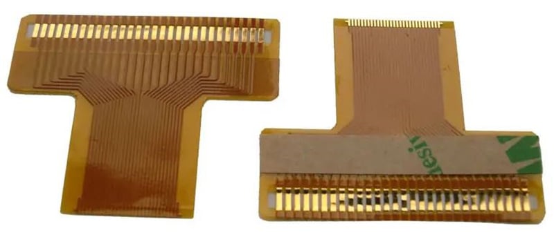
Dual access flex layer naming convention.
EMI Shielding Capabilities
A useful and cost-effective capability of a dual access flex PCB design that EMI shielding can be easily achieved on one or both sides of the design. The shielding is accomplished by using flex-specific EMI shielding films rather than adding additional copper ground layers. The shielding films are attached in the same manner as in a standard flex circuit. The circuit layout must have a ground circuit running throughout the design and preferably around the perimeter to create a Faraday cage configuration. We’ve covered the method of implementing EMI shielding in a separate blog but to summarize: the film has an electrically conductive adhesive that both laminates the film externally to the coverlay layers and electrically connects the shield layer through selective coverlay openings to the ground circuit.
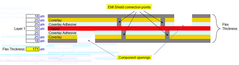
Dual access flex with EMI shielding film.
Summary
The unique construction of a dual access flex circuit and its capabilities can be advantageous to many flex circuit applications. Please feel free to contact Epec to discuss your specific needs and to have your design requirements reviewed to ensure the effectiveness of your design.
Key Takeaways
- Dual Access Flex Circuits Enable Two-Sided Component Access on a Single Copper Layer: These designs allow components or contacts to be placed on both sides without the need for multiple copper layers, making them ideal for tight bends and space-constrained applications.
- Ideal for ZIF-to-ZIF and Straight-Through Designs: Dual access flex is especially effective in designs where zero insertion force connectors or soldered components are required on opposing sides of the circuit, particularly when maintaining a straight pin-to-pin configuration.
- Manufactured Using Custom Coverlay Openings: The dual access construction involves machining different pad openings into coverlay layers on both sides of a single copper layer, creating independent access points for top and bottom connections.
- Design Constraints Mirror Single-Layer Flex Limits: As a one-layer design, signal routing is restricted with no crossing traces or multilayer via options. However, copper can be selectively exposed on both sides, provided the thickness and pad size meet mechanical strength needs.
- EMI Shielding Can Be Added Without Additional Layers: EMI shielding films with conductive adhesive can be applied to either or both sides of the flex circuit, offering effective electromagnetic protection without complicating the core circuit design.


