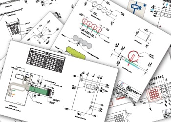
Printed circuit board (PCB) production has used standard panel sizes, such as 18x24 inches, to produce multiple PCBs at the same time, along with several other panel standards. A panel containing single format PCBs typically would use routing as the method of removing the single pieces from the master size.
Using the method of scoring came later, and then a combination of both v-score and rout was introduced. As larger equipment was developed, large panels became more widely used to produce printed circuit boards.
Two Methods of PCB Master Panel Setup
V-scoring is the method of passing a printed circuit board master panel between 2 blades simultaneously. As the blades are stationary, the PCB passes through the rotating blades, cutting both sides at the appropriate depth and angle. The table the PCB is firmly attached to is programmed to cut at specified dimensions. The scored path leaves a “v” grove on both sides of the master for ease of breaking.
Routing a circuit board is also a programmed mechanical process where the profile of the PCB is cut from the panel using a rotating router bit. The router is plunged into the waste laminate with the edge of the bit aligned to the edge of the circuit board’s desired size. The rout program is a combination of X and Y coordinates allowing the cutter to remove the PCB at the finished size and shape required. The routing process is time-consuming and can lead to delays or bottlenecks in the process.
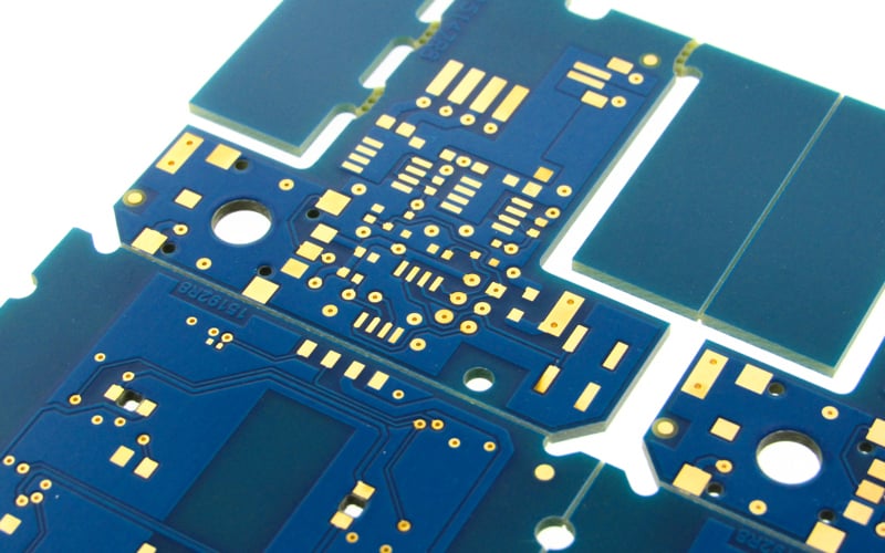
Combination of scored and routed circuit boards in an array.
PCB Panel Stability
Scoring a circuit board, unlike routing has certain criteria that must be considered to allow for manufacturing through the score process, a PCB must be comprised of straight-line cuts ending on a right angle. There cannot be any angles or radiuses along the scored axis. All angles or radiuses must be routed there for adding steps to the process to remove the PCBs from the master panel.
The circuit board also must not exceed a certain overall thickness for the card to be successfully scored typically 0.028” - 0.128” is the minimum/maximum overall thickness for a PCB to be scored. The material left behind from the score process is called a web. This extra material will hold the parts in the master panel until they are manually broken out.
Routed parts that are not in a single format either have waste rails or are in an array stepped with additional parts. The PCBs are held in place using a breakaway tab, the waste material is routed and skipped about 0.100” in length and pierced by holes, more commonly known as “mouse bites”. These tabs are non-plated holes to allow breaking.
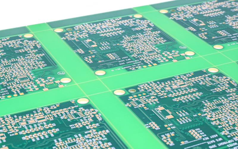
Scored circuit boards in an array.
The Issue with Both Processes
If the printed circuit board is in a single format or multiple parts per array, the score blades are cut from the top and bottom side to a specified depth leaving behind a web of uncut material. The perforated marks allow for the material to flex and bend for ease of breaking. If you cut too deep the parts will come apart without assistance from human hands leaving single pieces impossible to assemble.
If the cuts are not deep enough the bending and flexing may not be enough to break the parts out, causing manual assistance or rework to allow for separation of the pieces. Fully assembled parts cannot be reworked due to the components applied. Even the perfect scored parts have their challenge of a rough edge. The fiber-glass roughness is an irritant to the skin as well as a messy appearance. The waste material between scored parts must be greater than 0.200” for ease of breaking; less than 0.200” is difficult to snap.
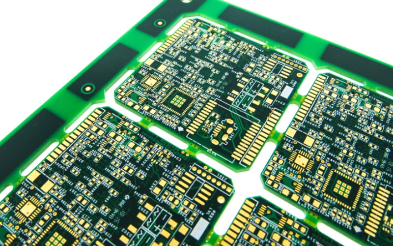
Routed circuit boards in an array.
Unlike scored, routed parts have a smooth finish, and although the dust from routing is an itchy waste product, the parts are cleaned prior to shipping to not pose a problem to the skin. The mouse bites can be the issue here, too big, or too close together and they can break like the score; too small and too few can leave bending the parts with fracturing into the board areas.
The larger problem like scoring, the broken tabs protrude away from the smooth actual edge. These rough areas can be sharp when handling, and they could pose an issue in fit to casings depending on the fit. To smooth the area, it requires manual sanding that is difficult to do after the assembly process.
Regarding materials for both methods, it should be mentioned that the higher Tg materials 170-180 are harder to break than standard Tg materials. Process adjustments must be made to allow for ease of breaking after assembly.
Summary
Considering the circuit board size, thickness, shape of the profile, and your assembler’s needs are key to a smooth transition from raw PCB manufacturing to full assembly. Scoring, routing, or a combination of both can be determined by your supplier for the best fit for production yield per master panel. Discuss your options with our engineering team here at Epec through our always-free DFM process prior to production.
Key Takeaways
- Two Main Separation Methods: PCBs can be separated from a master panel using v-scoring or routing. V-scoring uses angled cuts on both sides to create breakable grooves, while routing uses a rotating bit to cut profiles, often combined with scoring for complex shapes.
- Scoring Limitations: Scoring only works for straight-line cuts ending at right angles. It cannot be used for curves or radii, which must be routed instead. PCB thickness must also fall within the range of 0.028” to 0.128” for successful scoring.
- Edge and Handling Issues: Scoring leaves behind a fiberglass “web” that holds the parts together until broken out. If cuts are too deep, parts can fall apart prematurely; if too shallow, separation is difficult. Even properly scored edges can be rough and irritating to handle.
- Routing Considerations: Routing provides smooth edges but creates dust and “mouse bites” from breakaway tabs. If tabs are too large, edges protrude; if too small, boards can fracture. Smoothing sharp edges often requires manual sanding, which is difficult post-assembly.
- Material Impacts Breakability: High Tg PCB materials (170–180°C) are harder to break than standard Tg materials, requiring process adjustments during scoring or routing to ensure clean separation.


