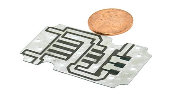
A printed circuit board (PCB) is an inexpensive and compact way to create many of the necessary interconnects between RF components in a subsystem. The interconnects are most often created with stripline and microstrip transmission lines, as well as vertical coaxial transmission lines created with plated through hole patterns.
There are many Microwave/RF PCB laminate materials available and it can be confusing trying to decide on the best raw material for a given RF design. For each material, the supplier generally provides a specification sheet, listing the various properties of the material. Use this post as a guide for navigating typical spec sheets of materials. It can be applied when selecting core materials, as well as the binding prepreg materials that hold the cores together.

Printed Circuit Board for RF Component
Dielectric Constant
The dielectric constant (Dk) or more properly, relative permittivity of a material is typically the first metric in consideration of which material to use for a given design. It is commonly notated as Dk or εr. Permittivity measures the electric field between charges within a dielectric and relative permittivity is a ratio of the absolute permittivity of a dielectric to the absolute permittivity of charges in a vacuum. Therefore, the relative permittivity of a vacuum dielectric is 1.0 Dk. Some common dielectric material Dk metrics are shown in the table below.
The higher the dielectric constant of a material, the greater the dielectric loss factor. However, larger dielectric constants will change the signal propagation velocity.
| Common Material Dks | |||
|---|---|---|---|
| Ceremics | 10+ | ||
| Rubber | 7.0 | ||
| Reinforced Teflon PCB Material | ~3.0 | ||
| PTFE | 2.1 | ||
| Air | 1.001 | ||
| Vacuum | 1.0 | ||
Dissipation Factor
Dissipation factor is also referred to as loss tangent, dielectric loss, or tan d (tan delta). It is a measure of the predicted insertion loss due to the dielectric carrier which the transmission line circuitry is printed on.
Total insertion loss is made up of four components:
- Reflective Loss: The geometries in the transmission lines and transitions in the circuitry create reflections at certain frequencies. Reflected signals exit the circuit at the input and are not transmitted and contribute to total insertion loss.
- Resistive Loss: The contours and surface roughness and the conductivity of the metals printed on the dielectric create resistive insertion loss, dissipating portions of the input signal as heat.
- Radiative Loss: Some portions of the signal power can be radiated into free space or cross coupled into an adjacent transmission line. Radiative losses are highest in a medium like unshielded non-coplanar microstrip but can be a factor even in stripline.
- Dielectric Loss: Dielectric losses are due to the propagation of a signal in non-vacuum medium. The higher the dielectric dissipation factor, the more dielectric losses will contribute to total insertion loss. In modern very low loss dielectric materials created specifically for the formation of RF transmission lines, the dielectric loss component is very low compared to the metallic losses of the transmission line.
Available Copper
Each dielectric material is available for purchase clad in metal that can be partially etched away to form the building blocks of transmission lines. By far the most common metal used for foil cladding of dielectric material is copper.
Different materials have different options for copper cladding. The first choice the PCB manufacturer must make is the weight of the copper cladding. Typically, this is specified in ounces, which translates to ounces per square meter. ½ ounce copper cladding is approximately 0.65 thousandths of an inch thick and 1-ounce copper is approximately 1.3 thousandths thick. Effective copper weight will also increase in production if the foil layer is subjected to plating operations such as via formation or routed edge plating.
The other critical feature of the selected copper foil is the roughness of the copper. It is important to understand this parameter as it pertains to both the side facing the dielectric material and the side facing away from the dielectric. The material manufacturer will typically treat the side of the foil that will face the material to create the proper topology for the bond strength they need. Bond strength is dependent on the surface area of the mating face of foil.
The two main styles of copper are listed below with some exploration into subtypes:
- Rolled Copper: Traditionally the smoothest copper option. Dielectric material manufacturers create this foil by taking copper bar stock and passing it through sequentially narrower rollers, a very smooth copper is created. This can be very helpful for low-loss applications but there can be some drawbacks. Rolled copper is more expensive to produce and drives up raw material costs. Also, if the surface against the dielectric is too smooth, then the peel strength of the copper can be too low, and it can release under temperature and stress (copper and dielectric materials don’t grow at the same rate when subjected to heat).
- Electrodeposited Copper: This foil is created by rotating a drum partially inside a plating tank while copper is slowly and continuously added to the drum. Two different levels and kinds of surface roughness are created on the two sides of the foil – against the drum and against the solution and air. Traditional, high profile ED copper has very good adhesion properties, both to the core material and to the PCB manufacturer’s prepreg layers. However, it is far costlier than rolled copper. There are also many reduced profile options available at the various material suppliers. Lower profile foils require novel methods of creating surface areas to meet mechanical hold requirements to the dielectric core. However, designers often need the lower-profile copper to meet loss requirements.
Coefficient of Thermal Expansion
The coefficient of thermal expansion (CTE), normally listed in the three Cartesian axes, describes the rate at which the PCB material will expand and contract over change in temperature. It is particularly important in certain applications.
- High Power or Harsh Environments: Either condition could cause thermal expansion or contraction and could put strain on plated vias, copper adhesion, multilayer laminations, or laminated heatsink adhesion.
- PCB Construction: If the PCB manufacturer needs to submit the board to high temperatures to fabricate it, there could again be strain on all the mechanical components and bonds. High temperatures are sometimes necessary for layered laminations, particularly prepreg-free fusion bonding.
- PCB Layer-To-Layer Registration: Critical to couplers, and in particular high pass filters, the practice of broadside coupling through thin-core PCB material to create capacitors relies on tight registration in these capacitive areas. As more or less of the adjacent layers overlap, the coupling values will change and can fall out of spec at certain operating temperatures. Another area of concern would be when an accurate phase is needed. There are a wide variety of CTE numbers on low-loss RF/microwave materials depending on the base material and what fillers they may have for support.
Filler Material
There are several types and subtypes of filler materials that are used in dielectric construction at the material suppliers’ fabrications.
Woven glass adds some rigidity to typically soft materials and can also restrict thermal expansion. It is a common filler material for microwave materials. Bundles of fibrous glass are woven in a crosshatch pattern to create a structure which is then sandwiched between two or more layers of Teflon or another dielectric.
Drawbacks of woven glass include:
- Material becomes more anisotropic.
- Glass creates patchy Dk where there is no glass in the z-axis in places and double glass where the weaves overlap.
- Glass bundles are not spread out.
There are alternate styles of glass reinforcement where the glass bundles are spread flat so that all areas have double thick glass and the Dk variance over a panel is greatly reduced.
There are various types of particle fillers as well. Instead of long strands, these fillers are small particles. Different developments have shown different geometries of the fillers. These fillers allow for a steady Dk across a panel and the opportunity to select a nominal Dk for the material by mixing different ratios of fillers of low and high Dk.
Key Takeaways
- Dielectric Constant (Dk) and Dissipation Factor (Df) Are Critical for Signal Integrity: Selecting RF PCB materials starts with understanding Dk and Df values. A stable, low Dk ensures consistent signal propagation, while a low Df minimizes dielectric losses, both essential for maintaining high-frequency performance and reducing insertion loss.
- Copper Type and Surface Roughness Impact Performance and Cost: Choosing between rolled and electrodeposited (ED) copper affects both electrical performance and mechanical reliability. Smooth copper reduces signal loss at high frequencies but may compromise adhesion, while rougher copper improves bond strength but increases resistance losses.
- Thermal Expansion Can Affect Reliability and Precision: The Coefficient of Thermal Expansion (CTE) influences how materials behave under temperature changes. In high-power or precision RF applications, mismatched CTE can lead to layer misalignment, via stress, and phase instability, especially in multilayer or harsh environment designs.
- Filler Materials Influence Mechanical Stability and Electrical Consistency: Woven glass and particle fillers are used to enhance rigidity and control thermal behavior. However, fillers can introduce Dk variability if not properly selected. Advanced filler designs help ensure uniform electrical properties across the PCB panel.
- Comprehensive Material Evaluation Ensures Optimal RF PCB Performance: Interpreting datasheets goes beyond just Dk and Df. Engineers must balance electrical, thermal, mechanical, and chemical properties to select the right laminate for both core and prepreg layers. Early collaboration with PCB manufacturers can streamline material choices and avoid costly design pitfalls.


