A pure notch or band stop filter (also called band reject filter) works by creating a Voltage Standing Wave Ratio (VSWR) resonance over a narrow bandwidth. This creates near total reflection over that bandwidth, while having very little reflection in the surrounding pass bands. By the nature of their creation, these notch filters are typically narrow band. Bandwidth comes linearly with added resonators, increasing size and loss.
An alternative approach to band stop creation is to separately design a pair of high pass and low pass filters with overlapping rejection bands in the stop band of interest. These two filters can then be connected in parallel with a pair of Tee-junction elements.
Tee-junctions are a kind of power divider/combiner used in diplexers and multiplexers to separate the electrical paths of the different pass bands. The combined response is a summation of the high pass and low pass filter responses and results in a band stop filter that can be tuned in frequency at either -3dB passband point with little impact on the other passband. This filter can also be tuned for bandwidth without the addition of more poles to the high pass and low pass filter components.
Example Filter
A moderate specification was chosen as a stop filter in order to demonstrate the high pass/low pass parallel method. This specification is shown in the table below.
| Band Stop Spec | |||
|---|---|---|---|
| Spec | Freq | Parameter | Level (dB) |
| Passband 1 | 10MHz - 2.5GHz | S21 | >-1 |
| Stopband | 3.25GHz-4.25GHz | S21 | <-13 |
| Passband 2 | 5GHz - 9GHz | S21 | >-1 |
High Pass Component
A five section high pass filter was designed and tuned in Microwave Office to approximate the upper half of the band stop spec. The filter was simulated and tuned as an air dielectric stripline with broadside coupling capacitance at the input and output and between the two shorted stub resonators. The insertion loss of the tuned high pass filter with limit lines for the band stop specs is shown below in Figure 1.
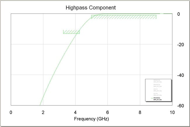
Figure 1: Insertion Loss of Tuned High Pass Filter.
Low pass Component
Like the high pass end, a five-section low pass filter was designed in air dielectric stripline with two open-circuit stub resonators separated by three matched transmission line sections. The low pass filter response is shown in Figure 2, along with the lower half of the band stop spec.
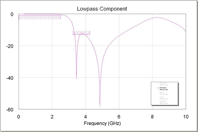
Figure 2: Low Pass Filter Response
Band stop Filter
The high pass and low pass components were connected in parallel by using tee-junctions on both sides of the filters. A tee-junction is a type of divider/combiner typically used in diplexers and multiplexers as a junction between the low pass and high pass arms. The resulting circuit required impedance tuning on both filters as well as an area near the tee-junction to achieve the high reflection stop band. Figure 3 shows the simulated insertion loss plot vs. the original band stop filter specs.
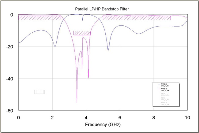
Figure 3: Band Stop Filter Simulated Insertion Loss
Tuning the LPF Over Frequency
To demonstrate the flexibility of tuning a band stop of this kind for frequency, a spec with the same high pass cutoff frequency, but a lower low pass cutoff frequency was selected, making a broader stop band. This is shown in the table below.
| Med. BW Band Stop Spec | |||
|---|---|---|---|
| Spec | Freq | Parameter | Level (dB) |
| Passband 1 | 10MHz - 2.0GHz | S21 | >-1 |
| Stopband | 2.75GHz - 4.0GHz | S21 | <-13 |
| Passband 2 | 5GHz - 9GHz | S21 | >-1 |
The new low pass was simply scaled linearly with respect to starting and target cutoff frequencies. Resonator lengths and transmission line lengths were scaled by a factor of 1.2:1 and retuned, while the transmission line and resonator widths were not changed as the same characteristic impedance was desired. The resulting high pass filter response is shown in Figure 4.
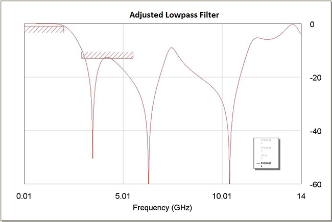
Figure 4: High Pass Filter Response
This filter was then stitched back into the bandstop filter as above, with some minor tuning for the high reflection stop band. The response to this new filter is shown in Figure 5.
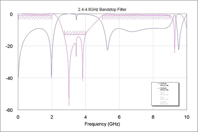
Figure 5: High Pass Filter Response After Tuning
Tuning the HPF over Frequency
Just with the low pass filter above, the high pass filter can also be tuned over frequency to change the center band stop frequency and the band stop bandwidth. To demonstrate this, a new spec was created with the same low-end specs as the second broader bandstop above and a higher high pass cutoff frequency, resulting in an even broader stop band. This spec is shown in the table below.
| Wide BW Bandstop Spec | |||
|---|---|---|---|
| Spec | Freq | Parameter | Level (dB) |
| Passband 1 | 10MHz - 2.0GHz | S21 | >-1 |
| Stopband | 2.9GHz - 5.5GHz | S21 | <-13 |
| Passband 2 | 6.7GHz - 10 GHz | S21 | >-1 |
The high pass filter was tuned similarly to the low pass, scaling the shorted stub resonators by a factor of 0.75:1, as well as the lengths of the couplers connecting them. The couplers had to be further tuned to compensate for the reduced coupling values of shortening their lengths. The resulting high pass filter response is shown in Figure 6.
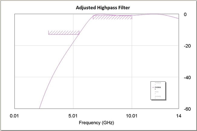
Figure 6: High Pass Filter Response After Coupler Tuning
The new high pass filter was then added back to the band stop model to create a band stop that is wider band both at the high pass and low pass ends than the original. The resulting model was tuned, and the response is shown in Figure 7.
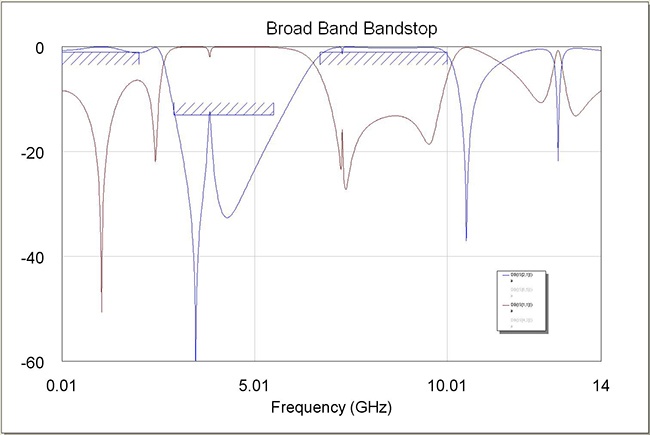
Figure 7: Wide Broad Brand Bandstop Filter Response
Summary
For challenging band stop applications, specifically those with a broad stopband or those that may require tuning in frequency of one band edge without much impact on the other, a parallel implementation of separate high pass and low pass filters may be a good solution. This solution allows the band stop edges to be implemented and tuned independently before being joined in parallel. Another benefit of the implementation is that broad band bandstop can be achieved without adding a loss and space-prohibitive number of resonators to the design.
Key Takeaways
- Traditional notch filters are narrowband: They work by creating VSWR resonance but require added resonators to broaden the stopband, which increases both size and loss.
- Parallel HPF + LPF approach enables flexibility: Designing high pass and low pass filters separately and connecting them with tee-junctions allows tuning of either passband edge with minimal impact on the other.
- Bandwidth tuning is more efficient: Scaling resonator and transmission line lengths in the LPF or HPF enables broader stopbands without requiring additional resonators, reducing loss and complexity.
- Tee-junctions provide effective integration: Acting as power dividers/combiners, tee-junctions combine the HPF and LPF responses, achieving high reflection in the stopband while maintaining strong passbands.
- Broader stopbands can be achieved with lower cost and size impact: Compared to conventional designs, this method allows wideband band stop filters with fewer resonators, less insertion loss, and better adaptability for custom specifications.


