


Mechanical bend reliability is a critical element in a successful flex or rigid-flex PCB design. One area that can have a significant impact is the transition line(s) that occurs from a rigid area, in a rigid-flex circuit design, or from a stiffened area, in a flex circuit with stiffeners design, to the flex layer(s) only areas.
This vertical linear change in the part’s construction thickness potentially creates a mechanical stress concentrator depending upon the bend requirements. If this situation occurs and is not addressed, it can cause the flex area circuits to be damaged when bent into the required shape.
This concern can be addressed in most designs by adding a strain relief preventing the flex layers from being bent beyond their physical capability. In this blog we will discuss why strain reliefs may be required, the materials used and design considerations that need to be applied.

Strain Relief
The purpose of a strain relief is to protect a part from stresses that can occur when it is bent or manipulated at a transition point within the design. The most common examples are wiring applications where a cable passes through an opening in an enclosure. If left unprotected the cable can be damaged or broken when bent or pulled against the hard edge of the enclosure opening. Strain reliefs exist in many formats from pass-through bushings, which protect against fraying at a hard edge, to over molds which force the cable to bend in a smooth arc preventing it from exceeding its bend capabilities and breaking or cracking.
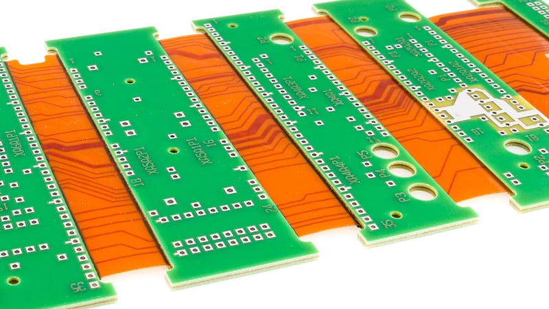
Rigid-flex circuit with selective epoxy strain reliefs.
Why Epoxy Strain Reliefs May be Required
A similar situation, as with wiring applications, can occur where the flexible circuit layers extend out from within the rigid areas of a rigid-flex or where a component area stiffener ends in a flex design. This combined with a bend requirement that is in close proximity to the transition can cause the flex layers to bend sharply rather than form a smooth radius. A sharp crease will exceed the minimum bend capabilities of the flex layer construction. This will cause the copper circuits to deform, work harden and lose ductility. If the flex layers are then straightened and or bent again there is a very high likelihood of the copper circuits cracking and creating either completely open or intermittent open connections.
A second reason for a strain relief is specified in IPC 2223 Design Standard for Flexible Circuits Section 5.2.9. Some rigid-flex designs may result in a small amount of pre-preg, used to laminate the rigid and flex layer together, extruding out from within the rigid layers onto the surface of the flex layers. Once cured pre-preg forms a hard sharp and slightly ragged edge. If left unprotected and combined with a bend requirement close to the transition, it can result in the flex layers being cut or torn when bent into position. While not all designs require strain reliefs it is very common to have them as a default requirement in high-reliability Class 3 designs.

Strain Relief Materials
A rigid-flex or flex circuit strain relief is created by adding a bead of a flexible material to the transition. When cured, this material creates a tapered fillet. The bead is applied using either a manual or pneumatically assisted syringe. This allows a relatively precise bead to be deposited right along the vertical edge of the rigid area or stiffener. The tapered shape combined with the material’s flexibility encapsulates any exposed pre-preg and forces the flex layers to take a smooth bend arc.
There are a variety of materials that can be used as a strain relief. While RTVs and silicone can be used the most common in the industry is Henkel Loctite’s Eccobond 45/15 two-part epoxy system. This system allows it to be mixed in different ratios which result in either a rigid, semi-rigid, or flexible material when fully cured. Only the flexible formula mix ratio can be used. The additional benefit of Eccobond is that it can withstand reflow temps. This allows it to be applied to the bare circuit before assembly by the flex circuit manufacturer. All other materials must be applied after assembly by the assembly facility as they cannot withstand re-flow temps.
Design Considerations
There are a few design requirements for the application of strain reliefs. The first item is the height difference between the surface of the flex layers and the surface of the rigid areas in a rigid-flex PCB design. A minimum of 0.010” is recommended to allow for sufficient space to apply the strain relief. This is driven by the viscosity of the material. If the strain relief is applied too thick, it may extend above the surface of the rigid area and then prevent the solder paste stencil from laying flush and creating assembly difficulties.
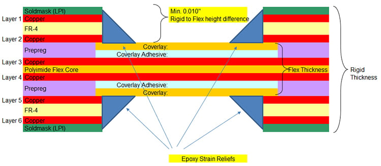 Minimum rigid to flex height requirement.
The second item is the length of the flex section connecting between rigid sections. The typical resulting width of a strain relief bead is between 1 - 2mm. The properties and viscosity of the material cause the material to run out on the surface of the flex layers. The typical min. manufacturable flex length is 3mm. If the strain relief is applied to both ends of a 3 - 4 mm long flex section, there may be insufficient flex length not encapsulated by the strain relief to meet the design’s bend requirements. In the worst case, the flex area may be completed encapsulated by the strain reliefs.
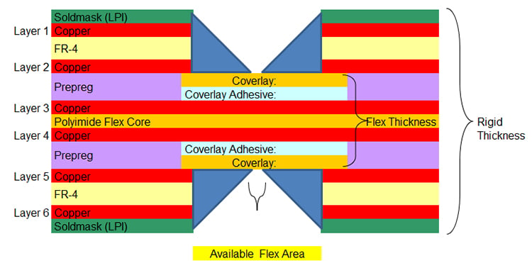
Restricted available flex area example.
Strain reliefs are typically applied to both sides of the flex layers at a specific transition location. In some unique applications, such as designs with unbalanced or offset flex layers in the construction, the strain relief can only be applied to one side of the flex layers due to insufficient height to the rigid area.
Summary
Flexible Epoxy Strain reliefs are an effective solution to many designs that ensure the mechanical bend reliability and prevent inadvertent damage to the flex circuit when installed in the assembly. Please feel free to contact Epec if you have any questions or require support in developing a rigid-flex or flex design to determine if it requires the addition of epoxy strain reliefs.
Key Takeaways
- Strain Reliefs Protect Critical Transitions: Epoxy strain reliefs are used at transition zones between rigid and flex areas to prevent mechanical stress concentrations, which can otherwise damage copper traces during bending.
- Required for High-Reliability Applications: While not all designs need them, epoxy strain reliefs are often specified in IPC 2223 for Class 3 high-reliability products, especially when pre-preg extrusions or sharp edges could compromise the flex layers during bending.
- Material Selection Is Crucial: Henkel Loctite’s Eccobond 45/15 epoxy is commonly used because it can be mixed for flexibility and withstands reflow temperatures, enabling pre-assembly application.
- Design Geometry Impacts Application: To ensure proper coverage and manufacturability, a minimum height offset of 0.010” is recommended between flex and rigid surfaces. Flex sections should be long enough to accommodate the 1–2mm wide epoxy bead without hindering bend function.
- Strain Reliefs Must Be Strategically Placed: Strain reliefs are typically applied to both sides of the flex area, but space constraints or design asymmetry may limit application to one side, requiring careful planning to avoid compromising flexibility.


