


Dating back to 1952, we are industry leaders and experts in all things printed circuit board (PCB) related, rigid PCBs, flexible circuits, and rigid-flex circuit boards combined, we know all the options and the difficulties in the fabrication processes. In this blog, we will focus on flex and rigid-flex PCBs what you should know and what to look for regarding the design and layout, as well as the importance of a successful data set and what is needed to prevent delays in engineering and manufacturing.

Flex and Rigid-Flex Circuit Board Terminology
Below are some common terms or abbreviations used in the flex and rigid-flex circuit board world. Some of these terms are common but some less common are worth a mention. The languages spoken across the world are changing, from the everyday talk as we knew it to the lingo. Talk-to-text, no matter where you live, we are seeing more shortcuts. To emoji and abbreviations used everywhere it is common to shortened text to make a point like, FPCB or RFPCBs to name a couple.
- FPCB: flex printed circuit board is a PCB that bends, flexes, and can twist to fit into a product.
- RFPCB: rigid-flex printed circuit board is a PCB that bends in a section or sections and has multiple rigid areas.
- Loose Leaf: refers to several flex areas that are not bonded together at the flex portion.
- Anchors or Tiedowns: are plated through holes within a flex area that are tear dropped for the stability of the flex areas, typically a mounting area.
- Tear Drops: are circuity built-up areas at circuit-to-pad interface that form the shape of a teardrop.
- Stiffener(s): are typically either polyimide or FR4 that are added to the flex area to aid in strengthening the flex for assembly of some sort.
- Cross-hatching: is a form of non-solid ground plane that aids in flexibility of the ground a solid area will not allow the flex to bend.
- PSA: is a pressure-sensitive adhesive and is applied to the flex or rigid-flex to allow bonding to the end product.
- Transition Zone: the area where the rigid material and flex materials meet or where the flex exits the center of the rigid stack of material.
Dos and Don’ts of Flex and Rigid-Flex PCB Data Sets
One of my favorite subjects regarding our printed circuit board manufacturing specialty is data. I love to look at data files. So, some of the dos and don’ts regarding the design of FPCB or RFPCB that should be considered early on in your design layout stage are critical to successful manufacturing in small or large volume. These rules will help you and your PCB supplier minimize fallout and the need for costly revision changes.
When it comes to flexible circuits of any type there are some additional parameters to consider. For starters, the shape of the part, where it will be used, the space that is needed to fit the part including length width and thickness after bending and flexing into the final shape. The outline(s), that is right more than one, are critical to engineering and productions success in building the part correctly. Don’t get me wrong in rigid circuit board manufacturing, the outline is very important as well but with flex and rigid-flex circuit boards the considerations are different.
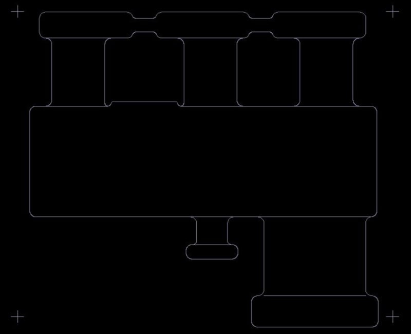
Example of a rigid-flex circuit board outline.
First, there can be many outlines, the overall, all-inclusive outline, the flex portion, or portions outline and the stiffener(s) outline. All important to your fabricator for ease of process and labeling them accurately.
The stack up of the part for all flavors of this unique process is a critical piece. When possible, leave the stack up for the fabricator to determine what is best for the product and advise your fabricator if there is an item pushing your product to a non-balanced construction. In the rigid circuit board world, we push for balance uniform construction with balance copper foil. The same is true for the flexible circuit board world where it is recommended to have the flex exit the rigid area from the center of the balanced layup.
Materials are not always available; if the type of material is not critical then leave that up to your supplier as well.
How Do Flexible Circuits Flex?
On your final product the flexible circuit bend radius maximum is 10x the thickness of the flex portion. Why is this important to the circuitry? For layout of the areas to be bent there should be no right angles in the trace layout, in fact using a smooth curve radius is what is best for producing the part and for bending the flex. Bending flexible circuits with sharp corners will cause the circuit to break in these areas, so smooth out those to curves.

Flexible circuit showing bend radius trace angles.
Regarding the traces, during layout stagger the traces from side to side on multilayers, staggering the traces will allow for the “thinness” to be maintained. Keeping the layers of copper tracks off each other from side to side will help keep the bend and thinness working together.
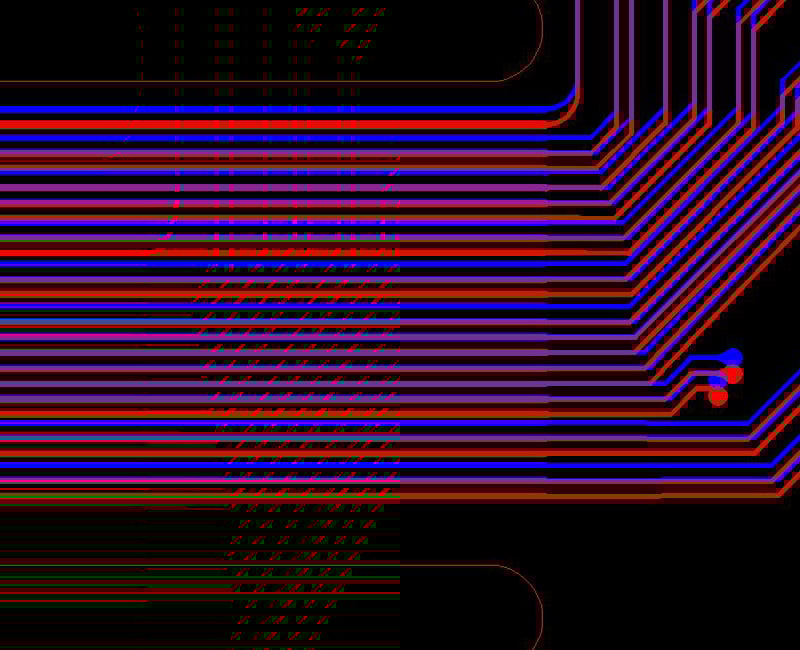
Flexible circuit designed with staggered traces.
As for holes, vias specifically, use as few holes as possible in the design. Keep in mind a 0.010” hole will need 0.010” annular ring and that the flex process needs more annular ring than the rigid. A 0.010” hole will need 0.030” copper pad to allow for sufficient annular ring. For the larger mounting holes used to attach the flex to the end product, these large holes should also have 0.010” annular ring as well as teardrops to increase the pad to circuit integrity.
Rigid holes to flex bend area need to be carefully placed. All holed should be kept a minimum of 0.050” from the transition zone. Ground areas or polygons must be hatched, a solid plain pour will prohibit the parts bend so no solids.
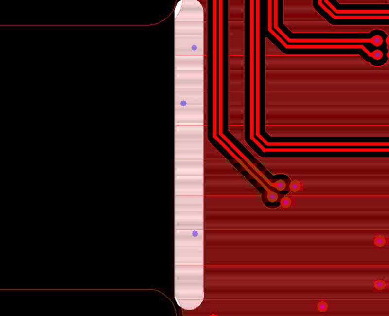
Example of transition zone from the rigid to flex areas.
All circuitry needs a coating of protection, whether it is a plating layer or a masking it is needed. The rigid-flex PCB may use both LPI, liquid photo imageable mask and what is known as a coverlay.
A coverlay is used on the flex areas, due to the bending of the part and the nature of coverlay and its flexibility. LPI has a much tighter control than coverlay does, however they both serve the same purpose to protect the copper from the elements, shorting or damage. Keeping in mind coverlay is routed and placed onto the surface and the openings must be much greater than the LPI mask. Allow for gang masking where mounting devices or components are being placed. Keep circuit to pad spacing at design rules that apply.
Always use a design for manufacturing (DFM) service to check and verify your data set for manufacturing. Finding issues upfront during the design and layout phase are time and cost savers. Our free DFM service is accessible on our website and available 24/7 to upload your data files. You will have a direct line to our engineering staff for a completed review, suggestions and correction needed prior to production.
When to Involve Your PCB Fabricator
Involving your PCB fabricator during design and layout stage is advantageous to ease of manufacturing. More often than not manufacturing is not considered at development which can lead to costly prototyping, re-spin of the data set and delays to market. With your circuit board fabricator involved early on to review and comment on the design and even perform a real time DFM it is always a win for both sides.
Summary
The main purpose of a flexible circuit board or rigid-flex circuit boards is to improve the integrity of the product while saving space or aiding in reducing the size of the final product. The cost can be up to 2 times that of a rigid circuit board or significantly more than a cable assembly, but the reliability from this product and the use of it is on the rise. Knowing how to properly design a rigid-flex PCB or flex PCB is key to your product's success, involving your supplier and its professionals is the best, quickest way to market.
For personal assistance in addressing your designs and options with a thorough design review and input from an experienced supplier. Please feel free to contact Epec if you have any questions.
Key Takeaways
- Precise outlines are critical: Multiple outlines (overall, flex portion, stiffeners) must be accurately defined for proper fabrication and labeling.
- Balanced stack-ups improve reliability: Letting the fabricator determine the best stack-up helps avoid unbalanced constructions and ensures better performance.
- Layout directly affects flexibility: Use smooth curved traces, staggered copper layers, and avoid vias near transition zones to maintain bend reliability.
- Protective coatings matter: Flex areas require coverlay while rigid areas use LPI mask, both essential to protect copper and ensure durability.
- Early collaboration saves time and cost: Involving the PCB fabricator early in design with DFM checks reduces errors, re-spins, and delays to market


